Semiconductor memory device and driving signal generator therefor

a technology of memory device and driving signal generator, which is applied in the direction of information storage, static storage, digital storage, etc., can solve the problem that continuous sensing operation consumes a large amount of sensing curren

Inactive Publication Date: 2001-05-29
SAMSUNG ELECTRONICS CO LTD
View PDF4 Cites 98 Cited by
  • Summary
  • Abstract
  • Description
  • Claims
  • Application Information

AI Technical Summary

Problems solved by technology

Such a continuous sensing operation consumes a large amount of sensing current.

Method used


Image

  • Semiconductor memory device and driving signal generator therefor
  • Semiconductor memory device and driving signal generator therefor
  • Semiconductor memory device and driving signal generator therefor

Examples


Embodiment Construction

The present invention now will be described more fully with reference to the accompanying drawings, in which preferred embodiments of the invention are shown.

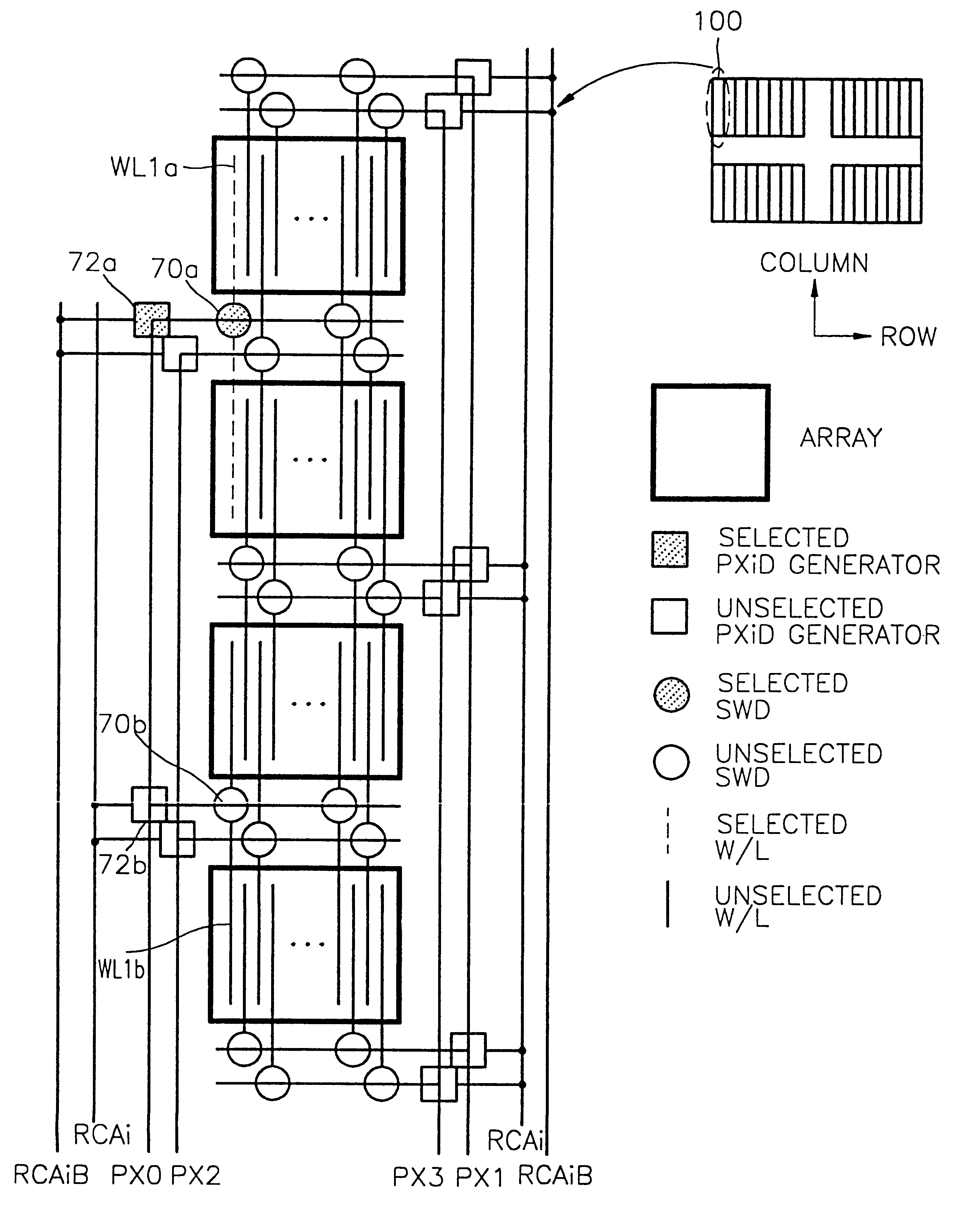
Referring to FIG. 3, during a normal operation, a semiconductor memory device according to a preferred embodiment of the present invention drives a portion of word-lines, hereafter referred to as "sub word-lines." Only sub word-lines connected to memory cells to be accessed are driven. Sub word-lines are word-lines W / L divided in a column direction.

In other words, doted lines represent word-lines W / L selected by row addresses. Among the word-lines W / L, the selected portions of the word-lines W / L, which are shown by solid lines, are enabled during the normal operation. The solid lines indicate sub word-lines connected to memory cells selected by column addresses. These sub word-lines are defined by segmenting the word-lines W / L in the column direction.

Referring to FIG. 4, a block diagram of a conventional decoder, once a row com...


PUM


Abstract

A semiconductor memory device is provided having reduced power consumption during a normal operation. The semiconductor memory device includes a sub word-line defined by segmenting a word-line and a driving signal generator for selectively driving the sub word-line according to a column address. The driving signal generator is controlled by a selection signal corresponding to the column address and a mode signal for specifying an operation mode of the semiconductor memory device. The semiconductor memory device enables part of the word-line according to the column address. The semiconductor memory device using a sub word-line driver to reduce the number of memory cells which are sensed, thereby reducing power consumption.

Description

1. Field of the InventionThe present invention relates to a semiconductor memory device, and more particularly, to a semiconductor memory device where power consumption is lowered by reducing the number of memory cells which are sensed by a sense amplifier.2. Description of the Related ArtDynamic random access memories (DRAM) are generally classified dependant upon their operation protocols. For example, a DRAM employing a mode of strobing addresses based upon row address strobe (RASB) signals and column address strobe (CASB) signals is commonly classified as an extended data output DRAM (EDO DRAM). A DRAM employing a mode of strobing commands, addresses, and data based upon clock signals may be classified as a synchronous DRAM. Yet another may be classified as a Rambus DRAM, which employs a mode of strobing commands, addresses and, data in the format of packets based upon clock signals (hereinafter, called a packet protocol mode).The former two types of DRAMs adopt an address multi...

Claims


Application Information

Patent Timeline
Patent Type & Authority Patents(United States)
IPC IPC(8): G11C8/00G11C8/10G11C11/407G11C11/401G11C11/406
CPCG11C8/10G11C11/407
Inventor LEE, JUNG-BAEYI, CHUL-WOO
Owner SAMSUNG ELECTRONICS CO LTD
Why Eureka
Try Eureka