In situ friction detector method for finishing semiconductor wafers

a technology of friction detector and semiconductor wafer, which is applied in the direction of grinding machine components, manufacturing tools, lapping machines, etc., can solve the problems of increasing costs, time-consuming, and adding extra expense to the operation, so as to reduce process yield and increase costs

Inactive Publication Date: 2001-09-04
SEMCON TECH +1
View PDF13 Cites 71 Cited by
  • Summary
  • Abstract
  • Description
  • Claims
  • Application Information

AI Technical Summary

Problems solved by technology

Although this can be done it is time consuming and adds extra expense to the operation.
Further the expensive wafers can be damaged during transfer to or from the measurement process further decreasing process yields and increasing costs.

Method used


Image

  • In situ friction detector method for finishing semiconductor wafers
  • In situ friction detector method for finishing semiconductor wafers
  • In situ friction detector method for finishing semiconductor wafers

Examples


Embodiment Construction

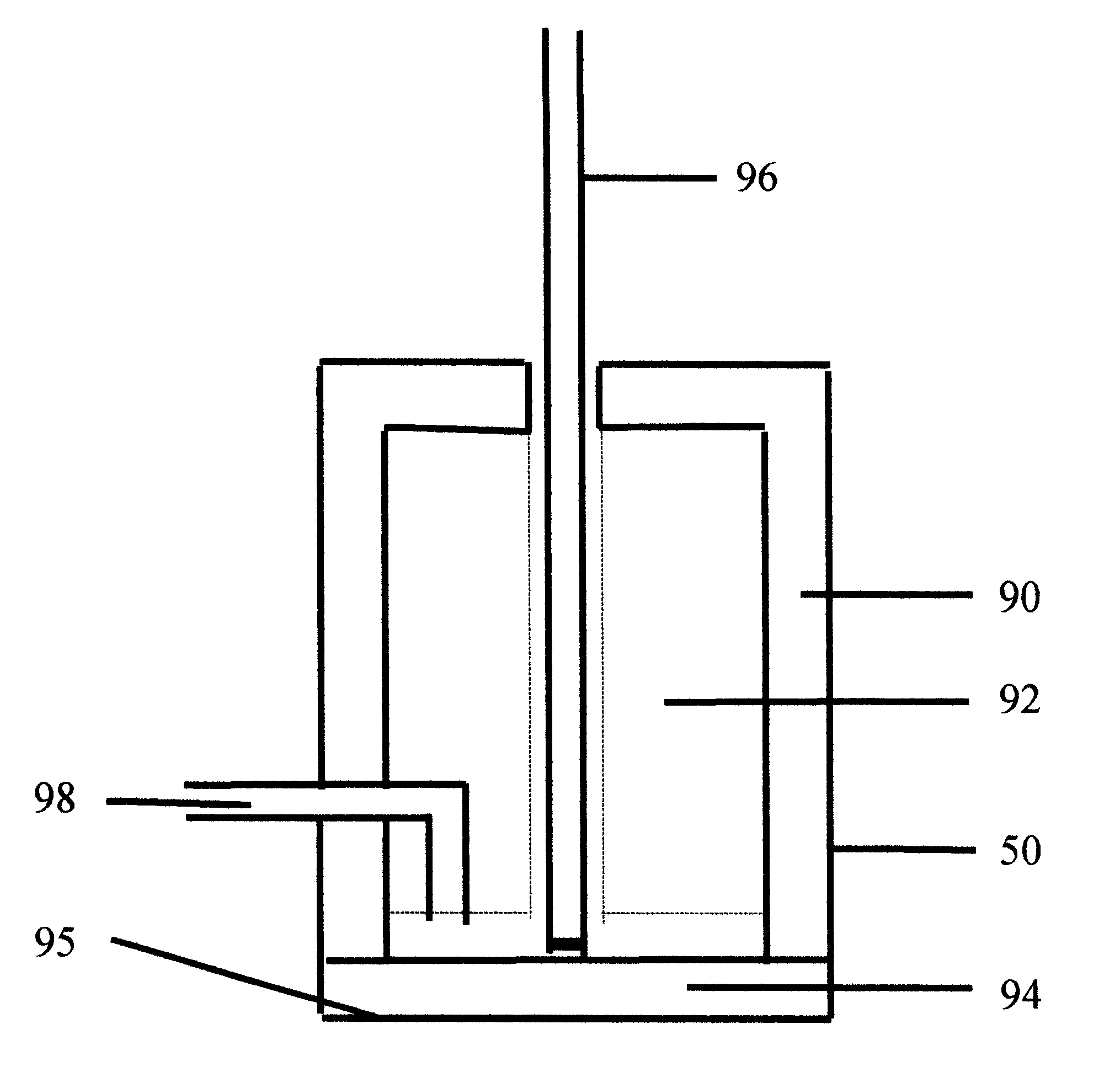
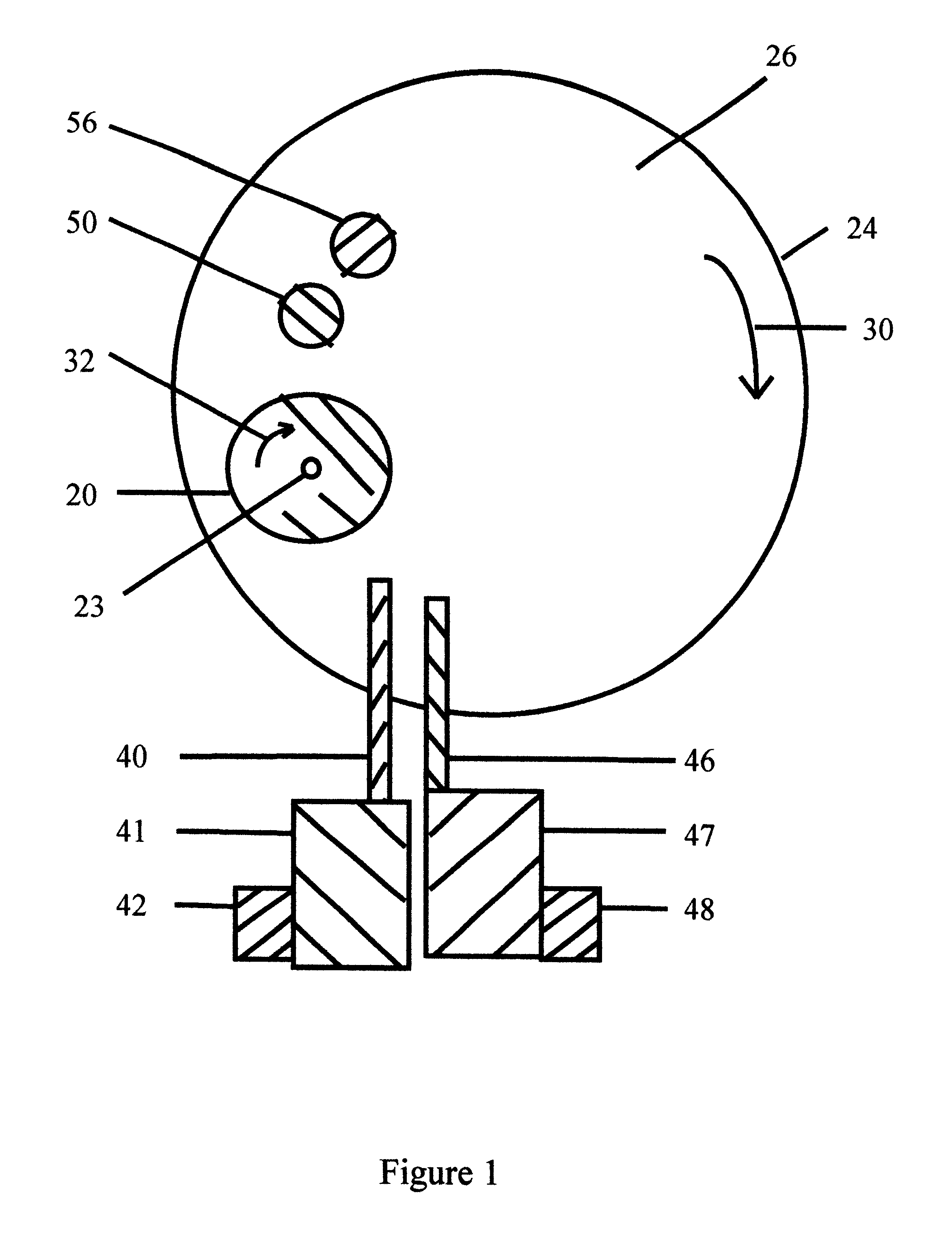
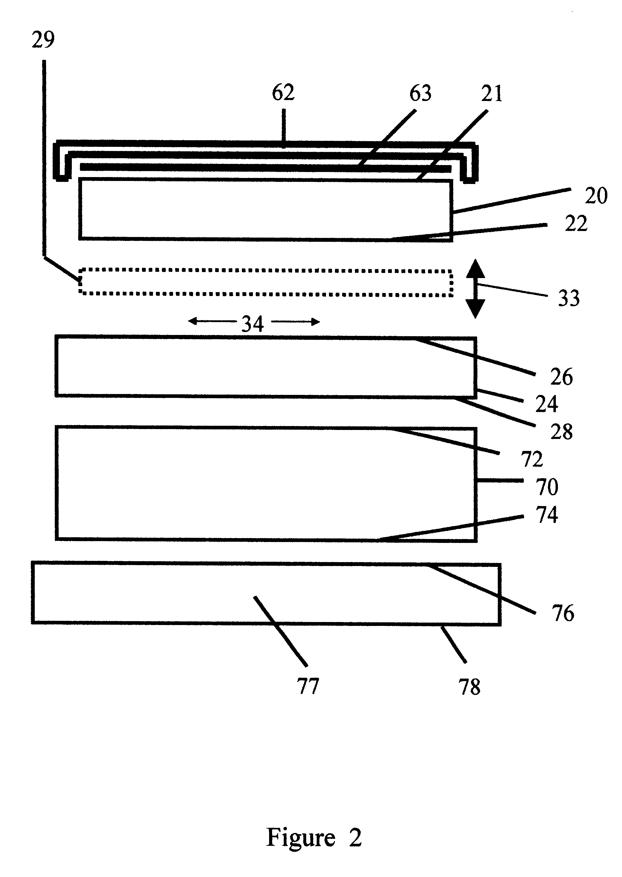
The book Chemical Mechanical Planarization of Microelectric Materials by Steigerwald, J. M. et al published by John Wiley & Sons, ISBN 0471138274 generally describes chemical mechanical finishing and is included herein by reference in its entirety for general background. In chemical mechanical finishing the workpiece is generally separated from the finishing element by a polishing slurry. The workpiece surface being finished is in parallel motion with finishing element finishing surface disposed towards the workpiece surface being finished. The abrasive particles such as found in a polishing slurry interposed between these surfaces finish the workpiece. FIGS. 1-5 are now discussed to better illustrate the invention.

Discussion of some of the terms useful to aid in understanding this invention are now presented. Finishing is a term used herein for both planarizing and polishing. Planarizing is the process of making a surface which has raised surface perturbations or cupped lower areas...


PUM


Abstract

A method of using of using a friction detector for finishing semiconductor wafers. The method uses secondary friction sensors which can interpolate and add improved control to finishing. The method aids control of finishing while using lubricating boundary layers in the operative finishing interface. The method aids control of differential lubricating boundary layers and improved differential finishing of semiconductor wafers. Planarization and localized finishing can be improved using differential lubricating boundary layer methods of finishing. Defects can be reduced using the in situ friction detector method.

Description

Chemical mechanical polishing (CMP) is generally known in the art. For example U.S. Pat. No. 5,177,908 to Tuttle issued in 1993 describes a finishing element for semiconductor wafers, having a face shaped to provide a constant, or nearly constant, surface contact rate to a workpiece such as a semiconductor wafer in order to effect improved planarity of the workpiece. U.S. Pat. No. 5,234,867 to Schultz et. al. issued in 1993 describes an apparatus for planarizing semiconductor wafers which in a preferred form includes a rotatable platen for polishing a surface of the workpiece and a motor for rotating the platen and a non-circular pad is mounted atop the platen to engage and polish the surface of the semiconductor wafer. Fixed abrasive finishing elements are also known for polishing semiconductor layers. An example is WO 98 / 18159 PCT application by Minnesota Mining and Manufacturing.Semiconductor wafer fabrication generally requires the formation of layers of material having particul...

Claims


Application Information

Patent Timeline
Patent Type & Authority Patents(United States)
IPC IPC(8): B24B49/04B24B49/16B24B49/02B24B37/04
CPCB24B37/013B24B37/042B24B49/16B24B49/04B65H2701/3772
Inventor MOLNAR, CHARLES J
Owner SEMCON TECH
Why Eureka
Try Eureka