High performance, low power vertical integrated CMOS devices

a cmos device, low power technology, applied in the direction of basic electric elements, semiconductor devices, electrical equipment, etc., can solve the problems of increasing the size and write time of the sram cell, increasing the delay of rc propagation, and other non-geometric solutions

Inactive Publication Date: 2001-10-02
INT BUSINESS MASCH CORP
View PDF42 Cites 73 Cited by
  • Summary
  • Abstract
  • Description
  • Claims
  • Application Information

AI Technical Summary

Problems solved by technology

However, reducing feature size alone may lead to problems that require other, non-geometric solutions, such as enhanced circuit wiring layers.
Unfortunately, these additional features increase SRAM cell size and write time.
's vertical FETs have substantial gate-drain and gate-source overlap with its associated overlap capacitance, which may be undesirable.
This overlap capacitance is part of circuit load capacitance and contributes to other performance problems, such as Miller Effects.
Furthermore, as feature size shrinks, wiring resistance (i.e., per unit line resistance) increases, increasing RC propagation delays, which offsets some performance gains.

Method used


Image

  • High performance, low power vertical integrated CMOS devices
  • High performance, low power vertical integrated CMOS devices
  • High performance, low power vertical integrated CMOS devices

Examples


Embodiment Construction

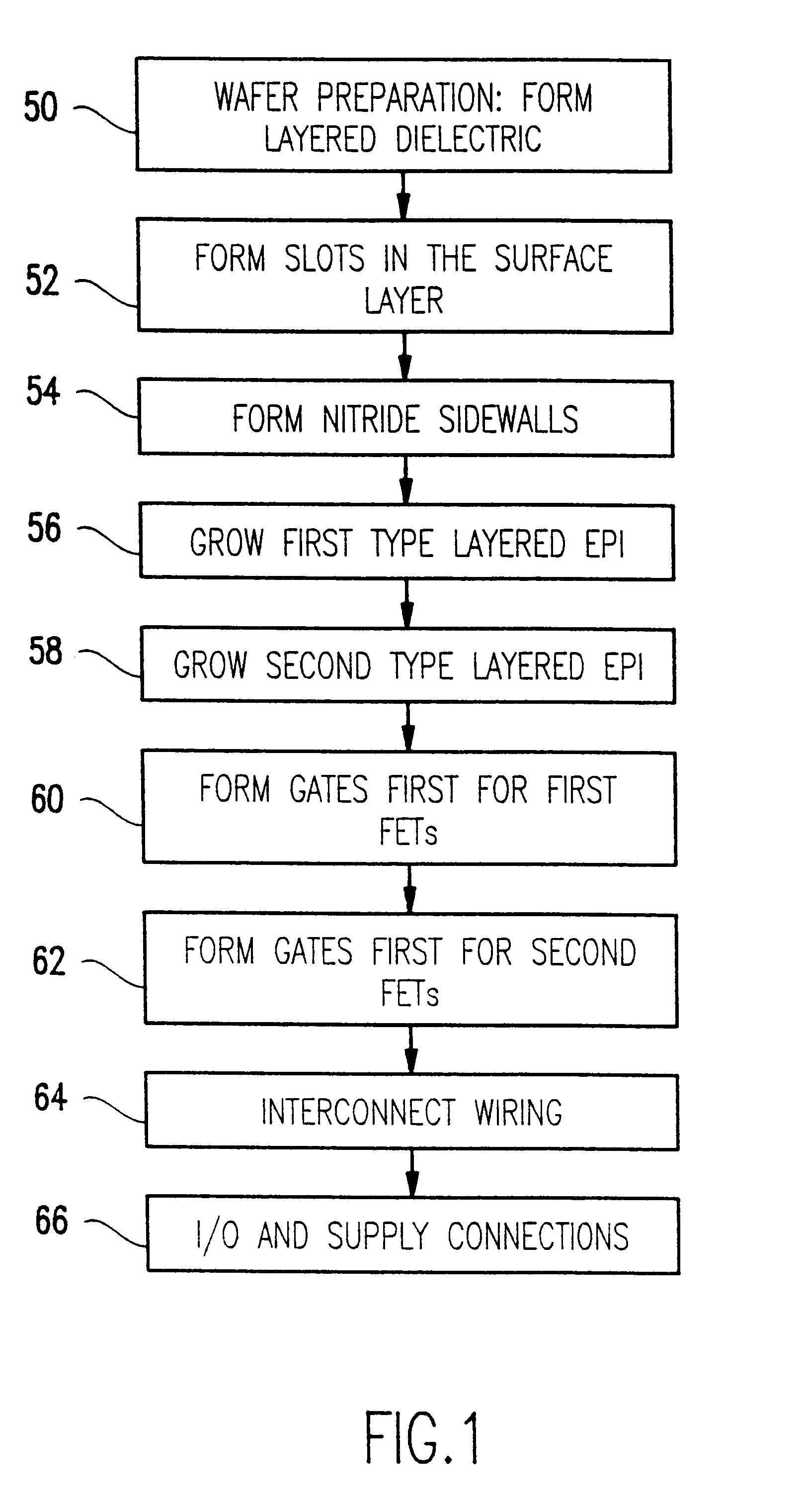
FIG. 1 is a flow diagram for forming FETs according to a preferred embodiment of the present invention.

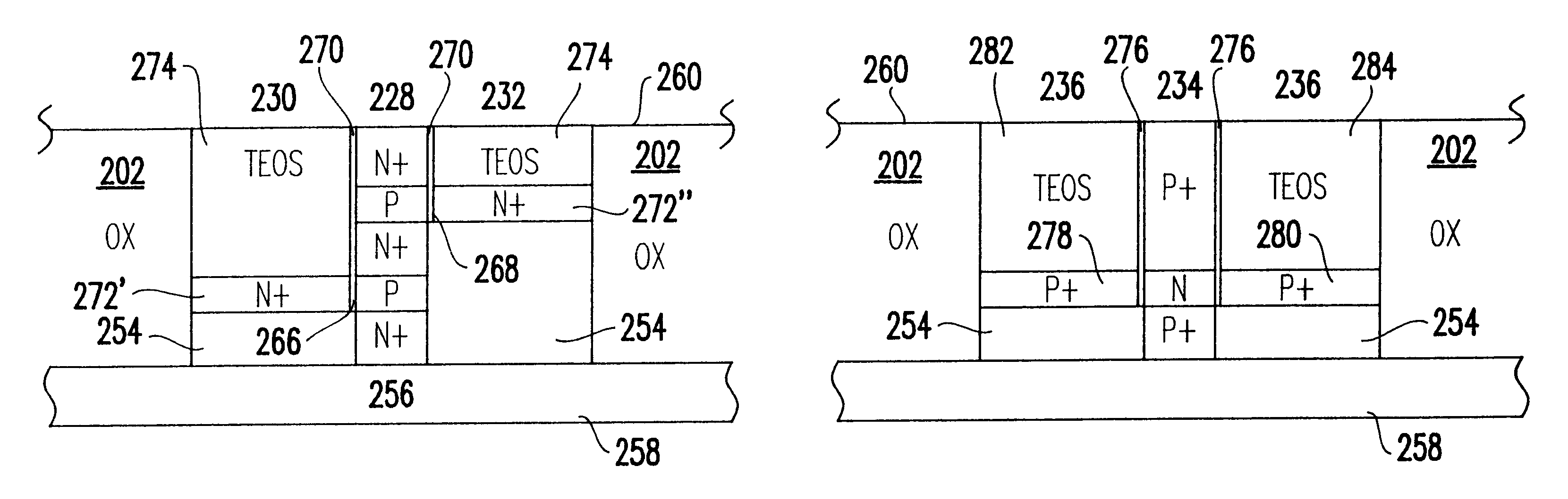
In its simplest form, the preferred embodiment of the present invention is a self-aligned vertical FET having both device characteristics and reduced device parasitic capacitance such as would normally be found in a self-aligned Silicon on Insulator (SOI) device. The preferred embodiment FET may be a short channel (0.1 micrometer (um)) N-type FET (NFET) or P-type FET (PFET). Complementary pairs of preferred self-aligned vertical devices (NFET:PFET) may be combined to provide CMOS equivalent circuits, e.g., a complementary pair of self-aligned preferred vertical devices (an NFET and a PFET) may be used as an inverter. Typical V.sub.h for a preferred embodiment circuit of preferred embodiment devices is <1.5V.

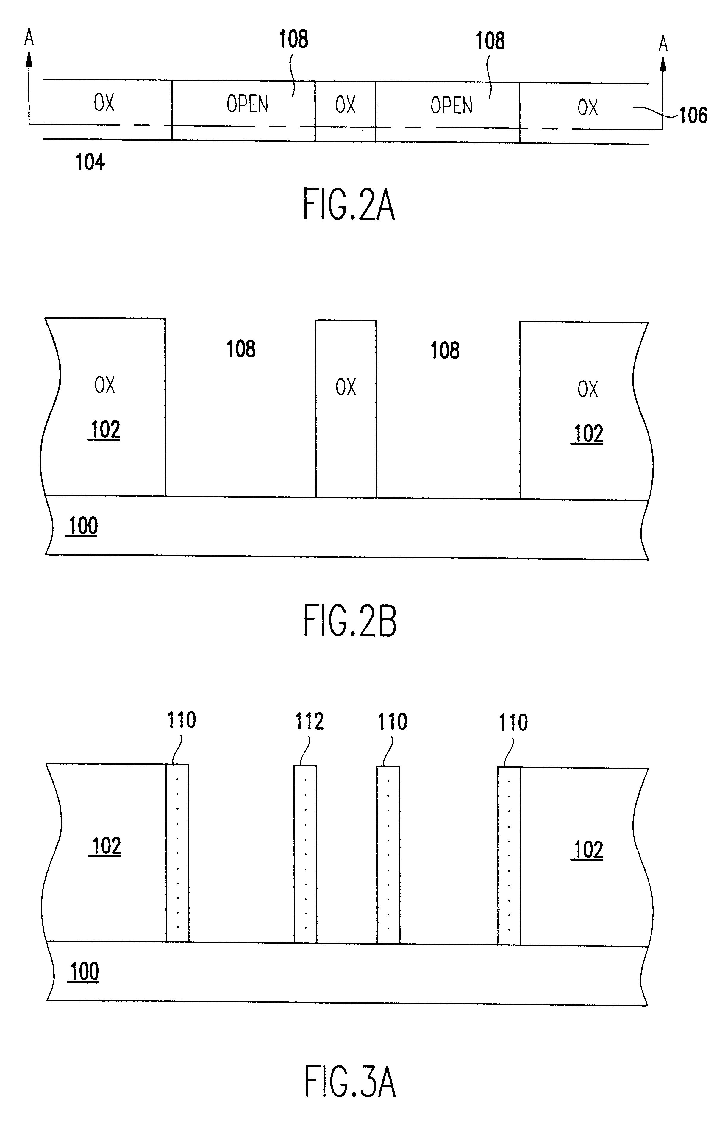
Preferred embodiment FETs are formed on the surface of a semiconductor wafer, preferably a silicon wafer. A layered dielectric is formed on a surface of the silicon wafer. Thus,...


PUM


Abstract

A vertical Field Effect Transistor (FET) that may be an N-type FET (NFET) or a P-type FET (PFET); a multi-device vertical structure that may be two or more NFETs or two or more PFETS; logic gates including at least one vertical FET or at least one multi-device vertical; a Static Random Access Memory (SRAM) cell and array including at least one vertical FET; a memory array including at least one such SRAM cell; and the process of forming the vertical FET structure, the vertical multi-device (multi-FET) structure, the logic gates and the SRAM cell. The vertical FETs are epitaxially grown layered stacks of NPN or PNP with the side of a polysilicon gate layer adjacent the device's channel layer. The multi-FET structure may be formed by forming sides of two or more gates adjacent to the same channel layer or, by forming multiple channel layers in the same stack, e.g., PNPNP or NPNPN, each with its own gate, i.e., the side of a polysilicon gate layer. The SRAM cell may be radiation hardened by selectively thickening gate layers to increase storage node capacitance, providing high resistance cell wiring or by including a multi-layered gate oxide layer of NO or ONO, or by any combination thereof.

Description

1. Field of the InventionThe present invention is related to integrated circuit (IC) chips and more particularly, to IC chips with CMOS SRAM cells and logic.2. Background DescriptionIntegrated circuit (IC) chip developers' primary goals are faster, denser, lower power IC chips. Typical, state of the art IC chips are manufactured, currently, in the complementary insulated gate Field Effect Transistor (FET) technology, commonly referred to as CMOS. Normally, each generation of CMOS technology is identified by its minimum feature size, e.g. {character pullout}half micron CMOS{character pullout} or {character pullout}quarter micron CMOS{character pullout}. Reducing the minimum feature size is the usual approach to making CMOS chips faster and denser simultaneously with reducing power.Since the active area (channel region) of any given circuit amounts to less than 10% of the entire area of the circuit, designers are acutely aware that, no matter how small a circuit is, circuit area may s...

Claims


Application Information

Patent Timeline
Patent Type & Authority Patents(United States)
IPC IPC(8): H01L21/70H01L27/11H01L21/8244H01L21/8238H01L27/12H01L21/84
CPCH01L21/823885H01L21/84H01L27/1203Y10S257/903H10B10/00H10B10/12
Inventor ARMACOST, MICHAEL D.BERTIN, CLAUDE L.HEDBERG, ERIK L.MANDELMAN, JACK A.
Owner INT BUSINESS MASCH CORP
Why Eureka
Try Eureka