Method of making higher impedance traces on a low impedance circuit board

a low impedance circuit board and high impedance technology, applied in printed circuit aspects, high frequency circuit adaptations, electrical apparatus construction details, etc., can solve the problem of increasing the characteristic impedance of all other signal traces on the insulation layer, reducing the thickness of the insulation layer of the signal traces, and increasing the cost of fabricating a pcb

Inactive Publication Date: 2002-08-13
INTEL CORP
View PDF8 Cites 45 Cited by
  • Summary
  • Abstract
  • Description
  • Claims
  • Application Information

AI Technical Summary

Problems solved by technology

However, reducing the thickness of the insulation layers of the signal traces can affect the characteristic impedance of the signal traces on the PCBs.
This, however, increases the thickness of an insulation layer thereby causing the characteristic impedance of all other signal traces on the insulation layer to be increased.
However, decreasing the width of the signal trace may significantly increase the cost of fabricating a PCB and may violate manufacturing standards.

Method used


Image

  • Method of making higher impedance traces on a low impedance circuit board
  • Method of making higher impedance traces on a low impedance circuit board
  • Method of making higher impedance traces on a low impedance circuit board

Examples


Embodiment Construction

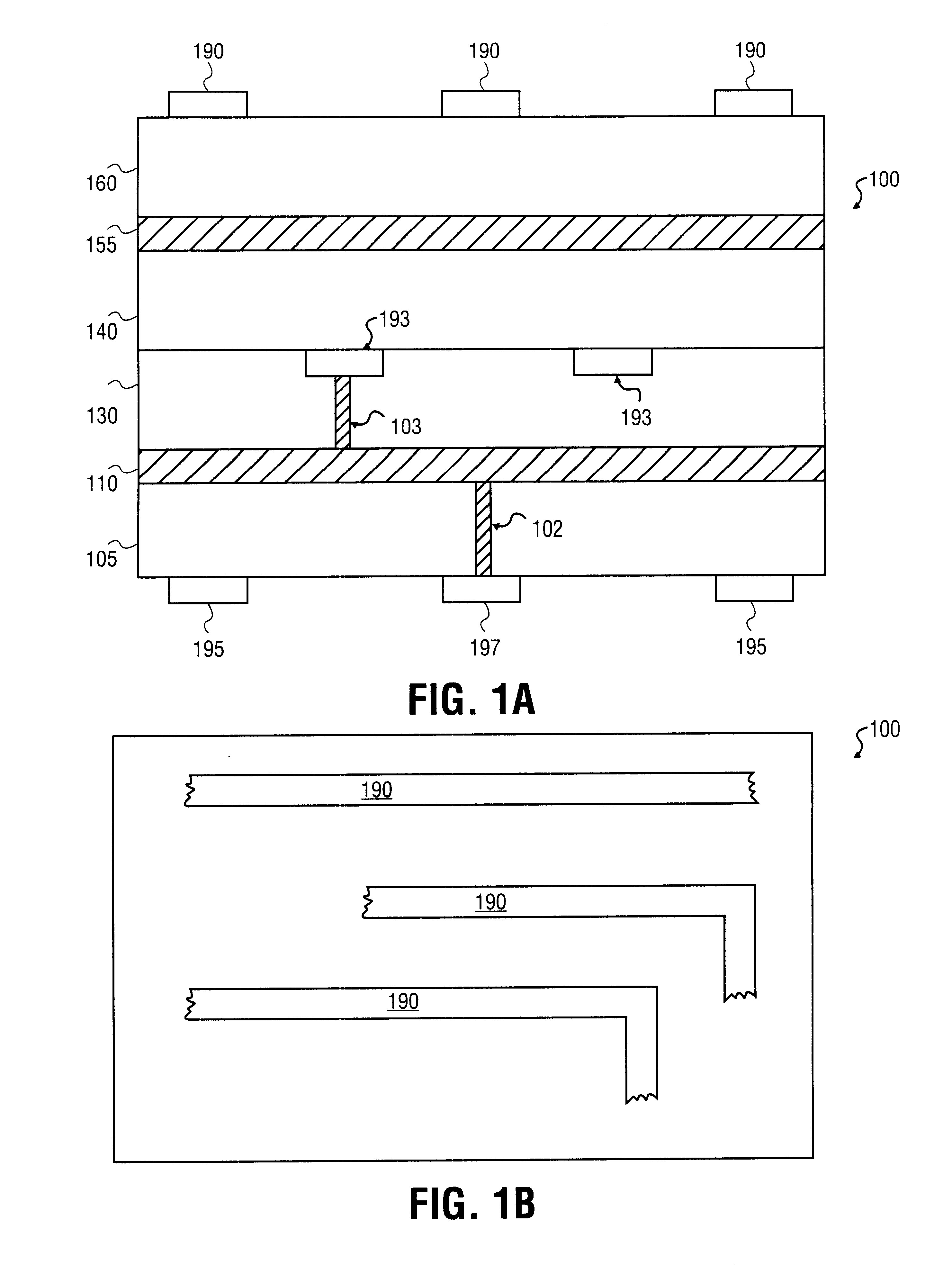
The present invention is a novel printed circuit board and method of making higher impedance traces on a lower impedance circuit board. A lower impedance circuit board refers to any circuit board having typical minimum size signal traces. In the following description numerous specific details such as specific materials, and dimensions, and processes are set forth in order to provide a thorough understanding of the present invention. One skilled in the art, however, will realize that the invention may be practiced without these specific details. In other instances, well-known circuit board manufacturing techniques and processes have not been described in particular detail so as to avoid unnecessarily obscuring the present invention.

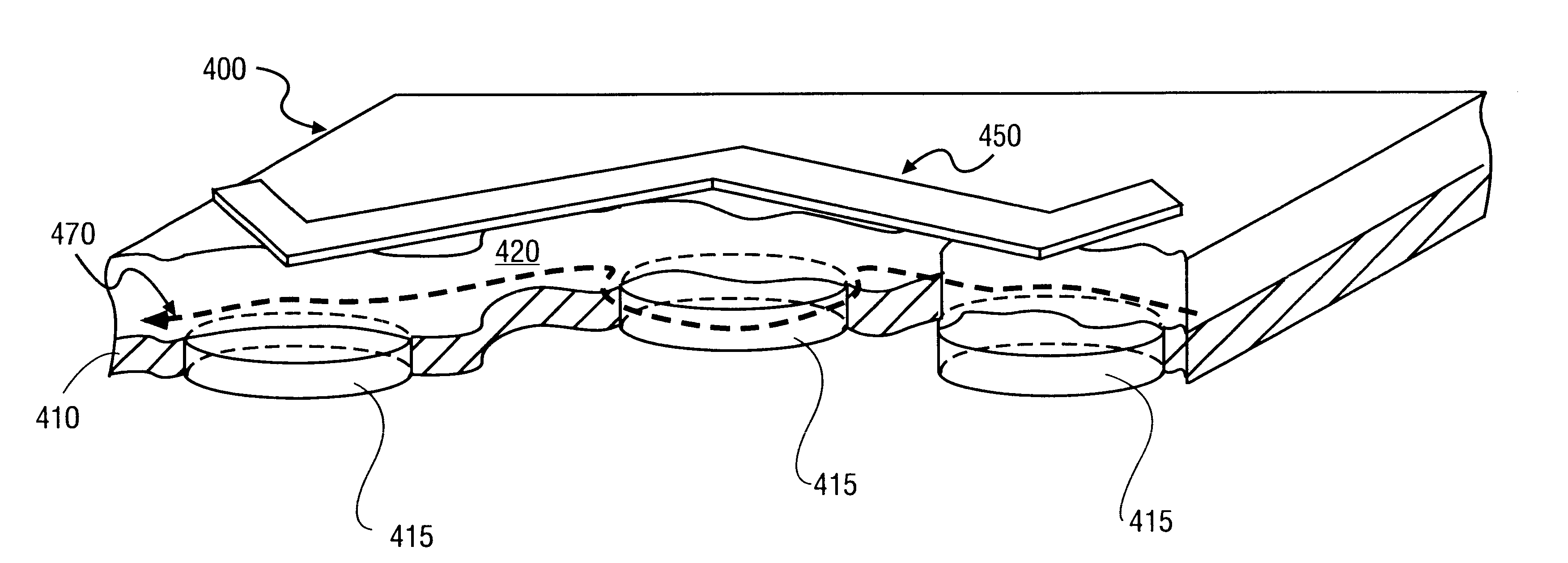
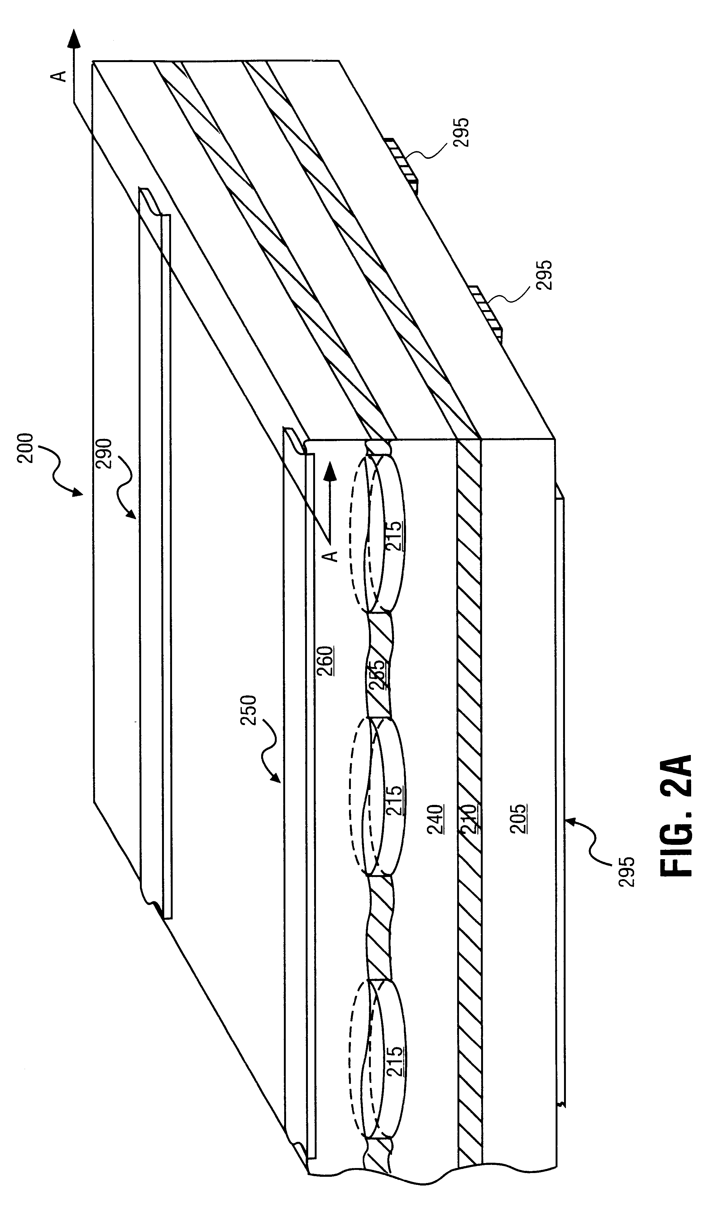
The present invention is a novel circuit board and methods of increasing the characteristic impedance of a signal trace by forming a plurality of voids along the length of the signal trace in the nearest conductive reference plane(s) directly below and / or ...


PUM

PropertyMeasurementUnit
impedanceaaaaaaaaaa
impedanceaaaaaaaaaa
impedanceaaaaaaaaaa

Abstract

The present invention is a circuit board having a plurality of voids in a conductive reference plane to increase the characteristic impedance of a signal trace. The circuit board of the present invention comprises a conductive reference plane having a plurality of voids formed therein, and a signal trace formed over the conductive reference plane.

Description

1. Field of the InventionThe present invention relates generally to the field of printed circuit boards ("PCBs"). More particularly, the present invention relates to a method of making higher impedance traces on a low impedance circuit board.2. Discussion of Related ArtThe common types of PCBs are a double-sided PCB and multi-layered PCB. A double-sided PCB includes conductive planes formed on the both sides of an insulation layer. A multi-layered PCB includes a plurality of conductive planes and insulation layers. In a multi-layered PCB, an insulation layer is typically formed in between conductive planes. The multi-layered PCB can have three or more conductive planes. The conductive planes refer to signal trace layers, power planes, or ground planes.FIG. 1A and FIG. 1B show a multi-layered PCB 100. FIG. 1A shows an illustration of a cross-sectional view of PCB 100. FIG. 1B shows an illustration of a top view of PCB 100 of FIG. 1A.Referring to FIG. 1A, PCB 100 includes signal trace...

Claims


Application Information

Patent Timeline
Patent Type & Authority Patents(United States)
IPC IPC(8): H05K1/02H05K1/00
CPCH05K1/0224H05K1/0253H05K1/0298Y10T29/49155H05K2201/09681H05K2201/0969H05K2201/093
Inventor DOBERENZ, PHILIP W.
Owner INTEL CORP
Why Eureka
Try Eureka