Method of performing parasitic extraction for a multi-fingered transistor

a multi-finger transistor and parasitic extraction technology, applied in the field of integrated circuit devices, can solve the problems of inability to accurately measure the parasitic resistance of multi-finger transistor devices, less space occupied by multi-finger devices, and inability to produce error-free approximation results, etc., to achieve the effect of reducing the delay of the signal traveling along the finger and affecting the model accuracy

Inactive Publication Date: 2003-02-11
IBM CORP
View PDF2 Cites 6 Cited by
  • Summary
  • Abstract
  • Description
  • Claims
  • Application Information

AI Technical Summary

Problems solved by technology

However, the multi-finger device takes up less space and has less resistance than the conventional transistor device of the appropriate width.
However, when the width of the fingers becomes too large, the error in the approximation produces unacceptable results.
More specifically, as the fingers become wid

Method used


Image

  • Method of performing parasitic extraction for a multi-fingered transistor
  • Method of performing parasitic extraction for a multi-fingered transistor
  • Method of performing parasitic extraction for a multi-fingered transistor

Examples


Embodiment Construction

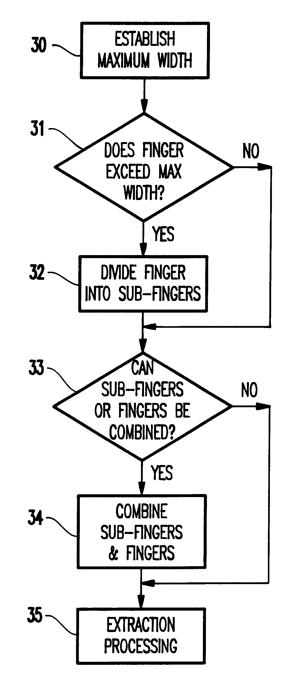
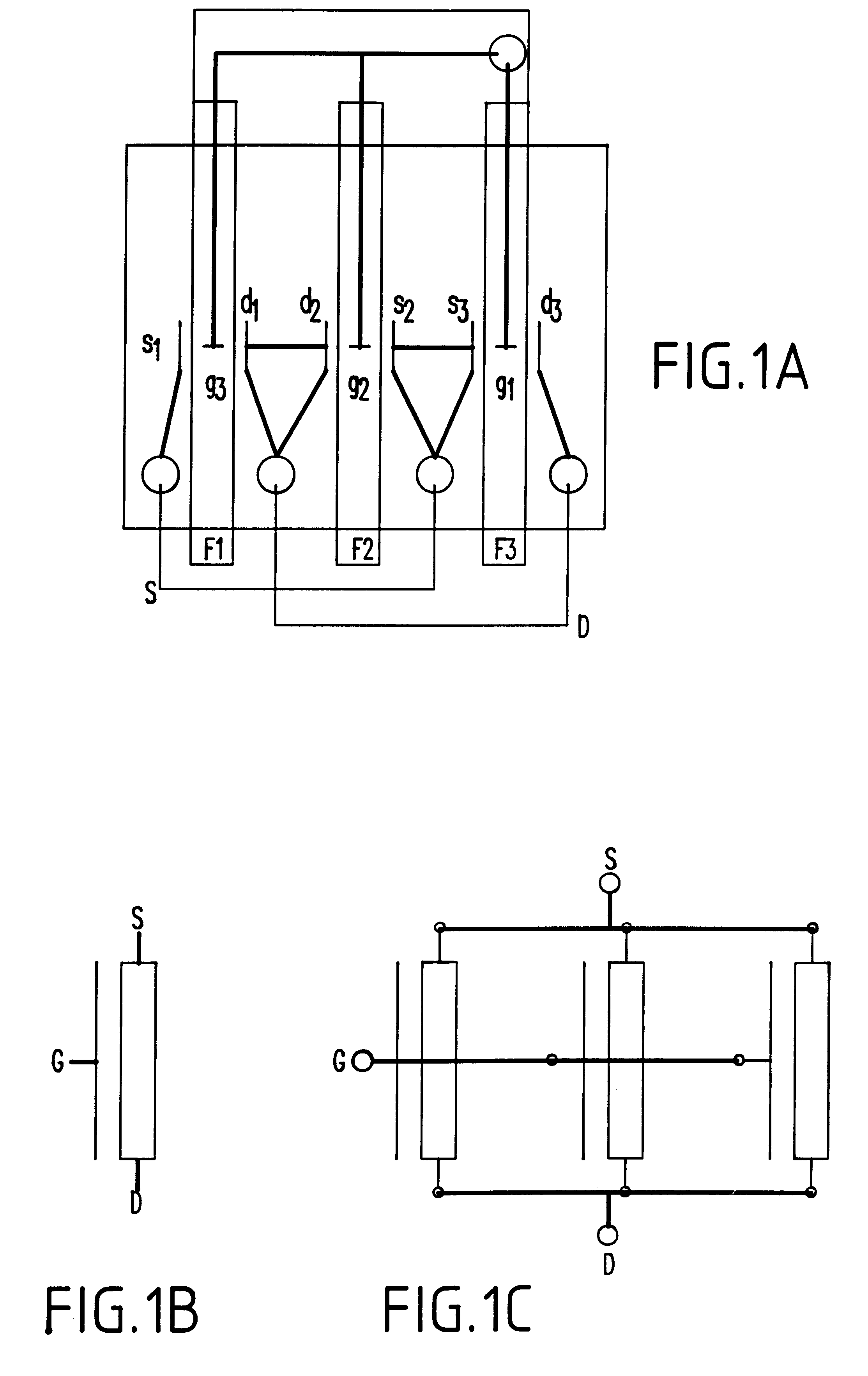
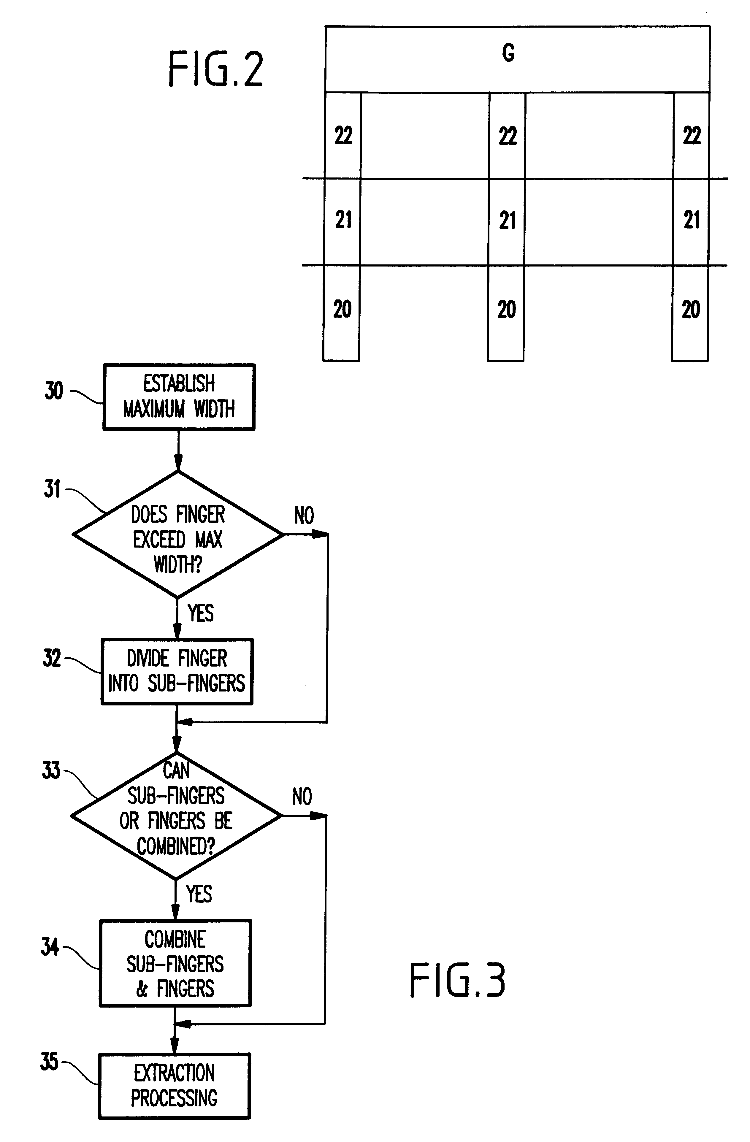
While conventional parasitic extraction tools rely on the user to consider (or usually ignore) device parasitic resistance in the device model, the invention supplies a method for extending the extraction and modeling capability of the extraction program to the resistors connected to the source, drain and gate of field effect transistors (FETs). With the invention the ports at which the resistors are connected to the device are situated in the middle of the gate for the gate contact. A short stripe is created under the sidewall of the gate poly to connect to source and drain resistors to the device. In this situation, each finger of a multi-finger FET device is connected with a different theoretical resistor network, which makes all fingers unique and separated in the netlist.

If the contact is only on one end of the device the voltage drop along the width of the device can require a break up of the device for accurate description of the device current.

Therefore, to achieve good accu...


PUM


Abstract

A method and structure for performing parasitic extraction for a multi-fingered device comprising of establishing a maximum processing width of a finger of the device, dividing fingers of the device that exceed the maximum width into sub-fingers, determining whether ones of the fingers and the sub-fingers have similar characteristics, combining ones of the fingers and the sub-fingers that have similar characteristics into combined fingers, and extracting parasitic values from the fingers, the sub-fingers and the combined fingers.

Description

1. Field of the InventionThe present invention generally relates to integrated circuit devices and more particularly to an improved system and method for measuring parasitic resistances on multi-finger transistor devices.2. Description of the Related ArtConventional transistor devices include a source, drain and gate. When current flows across the gate, a connection is either made or broken between the source and drain. Therefore, the transistor acts as a switch to connect or disconnect electronic components. Multi-finger integrated circuit devices include a single gate that is connected to multiple source contacts and multiple drain contacts. The multi-finger transistor performs the same functions as a conventional transistor (e.g., acts as a switch). However, the multi-finger device takes up less space and has less resistance than the conventional transistor device of the appropriate width. For these reasons (and others) the use of multi-finger transistors is increasing.The output...

Claims


Application Information

Patent Timeline
IPC IPC(8): G06F17/50
CPCG06F17/5036G06F30/367
Inventor BAKKER, WILLIAM C.DEWEY, III, L. WILLIAMHABITZ, PETER A.MCCULLEN, JUDITH H.SEIBERT, EDWARD W.SULLIVAN, MICHAEL J.
Owner IBM CORP
Why Eureka
Try Eureka