Driver of liquid crystal display

a technology of liquid crystal display and driver, which is applied in the direction of identification means, instruments, optics, etc., can solve the problems of increasing the number and the size of its drivers, raising the cost, and the connection between the drivers and the panel

Inactive Publication Date: 2003-02-25
SAMSUNG ELECTRONICS CO LTD
View PDF6 Cites 38 Cited by
  • Summary
  • Abstract
  • Description
  • Claims
  • Application Information

AI Technical Summary

Benefits of technology

The present invention relates to a liquid crystal display and, more particularly, to a driver of liquid crystal display, in which the driving signal applied to the two scanning lines adjacent to each other is controlled to allow one data line to send two video signal to both pixels, respectively, thereby reducing the number of the data lines by half in comparison with the conventional liquid crystal display.
To accomplish the object of the present invention, there is provided a liquid crystal display having first and second plates and a liquid crystal being sealed therebetween, including: a plurality of scanning lines arranged on the first plate in one direction; a plurality of data lines arranged on the first plate, intersecting the scanning lines; first and second pixel regions, located at both sides of each data line, respectively; a first switch for selectively transmitting a video signal loaded on a corresponding data line to the first pixel region; and a second switch for selectively transmitting the video signal loaded on the data line to the second pixel region.
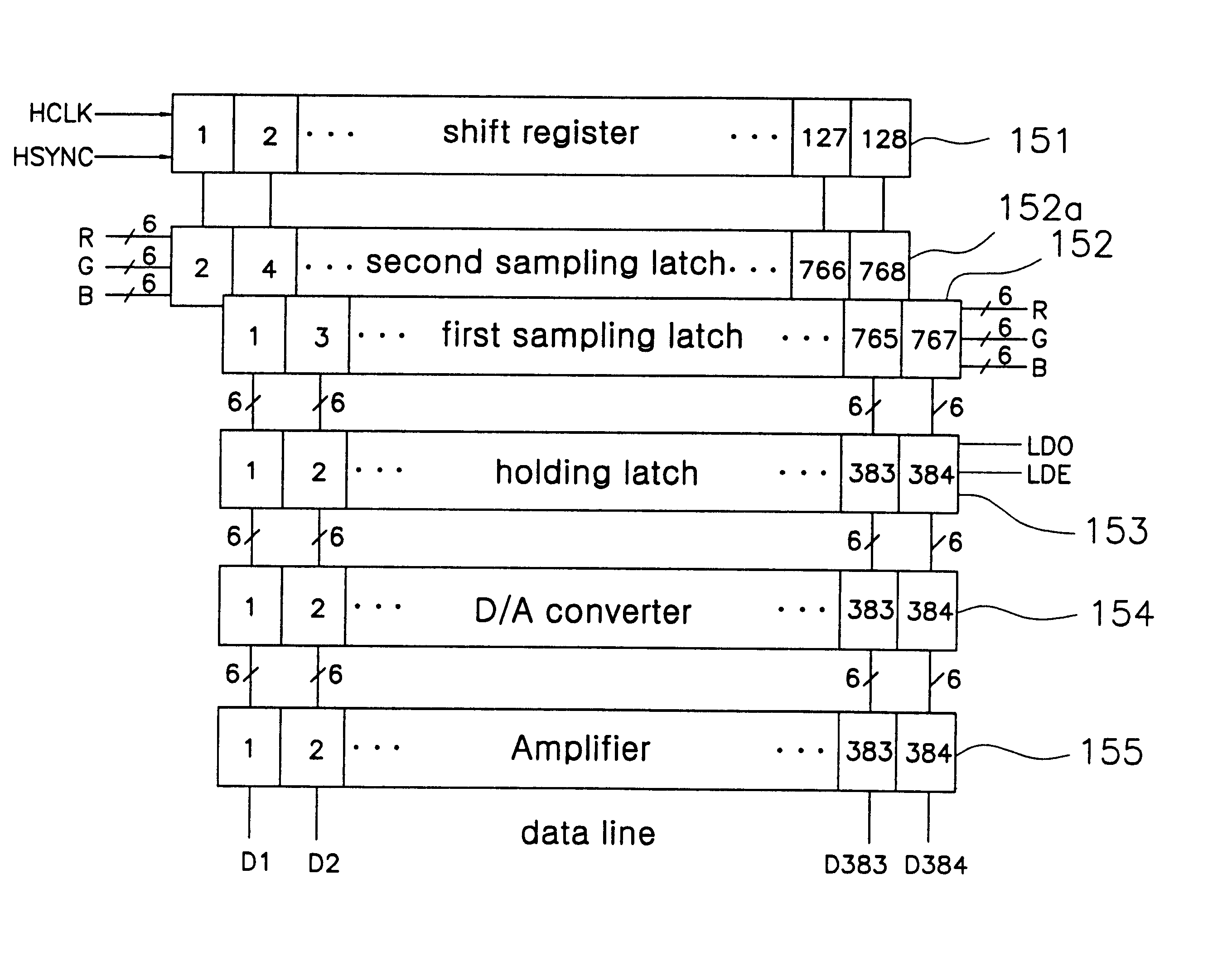
To accomplish the object of the present invention, there is also provided a source driver for driving a liquid crystal display, which includes: an n / 3-clock shift register for shifting a start pulse to output a latch clock; a first sampling latch for sampling and latching digital video signals corresponding to odd-numbered column lines among 2n column lines according to the latch clock sent from the shift register; a second sampling latch for sampling and latching digital video signals corresponding to even-numbered column lines among 2n column lines according to the latch clock outputted from the shift register; a holding latch for receiving and latching the data stored in the first sampling latch according to a first load signal, and for receiving and latching the data stored in the second sampling latch according to a second load signal; a D / A converter for converting the digital video signals corresponding to the odd-numbered column lines or the digital video signals corresponding to the even-numbered column lines, stored in the holding latch, into analog data signals; and an amplifier for amplifying the currents of the analog video signals corresponding to the odd-numbered column lines or the analog video signals corresponding to the even-numbered column lines, supplied from the D / A converter.
To accomplish the object of the present invention, there is also provided a gate driver for driving the liquid crystal display, which includes: a shift register for shifting a starting pulse depending on a gate pulse clock; a logic circuit for selectively receives a plurality of output signals of the shift register, logically operating them and outputting them; a level shifter for shifting the output of the logic circuit to a predetermined level, to sequentially output it; and an output buffer for sequentially applying the level-shifted signal to scanning lines.

Problems solved by technology

However, the aforementioned conventional liquid crystal display has the following problem.
In case where the number of pixels increases in order to realize a large-sized liquid crystal display with a higher resolution, the number and the size of its drivers also increase to raise the cost.
This brings about a new problem such as connection between the drivers and panel.

Method used


Image

  • Driver of liquid crystal display
  • Driver of liquid crystal display
  • Driver of liquid crystal display

Examples


first embodiment

FIG. 7A shows the configuration of a liquid crystal display according to the present invention. Referring to FIG. 7A, a plurality of scanning lines G1, G2, . . . , Gn-1, Gn are arranged in row direction whereas a plurality of data lines D1, D2, . . . , Dn-1, Dn a rearranged in column direction, intersecting the scanning lines. At the portion where each scanning line intersects each data line, first and second switches 71 and 73 transmitting a video signal are located at pixel regions placed on the left and right hands of the data line, respectively. First and second pixel electrodes 71c and 73c are respectively connected to the first and second switches 71 and 73. Here, each of the first and second switches is preferably configured of an N-type or P-type thin film transistor.

The configuration of the liquid crystal display of the present invention is described below in more detail with reference to the portion "X" of FIG. 7A. The first switch 71 located at the left side of a data lin...

second embodiment

In the liquid crystal display having the above-described configuration according to the present invention, upon application of a driving signal with the waveform of FIG. 8B to the scanning lines, an image is displayed, moving from the upper part to the lower part of the liquid crystal panel, and a corresponding data line delivers the video signal to the pixels located at the left and right sides thereof, resulting in reduction in the total number of the data lines.

FIG. 9A shows the configuration of a liquid crystal display according to a third embodiment of the present invention, and FIG. 9B shows the waveform of a driving signal applied to the scanning lines of the liquid crystal display of FIG. 9A. Referring to FIG. 9A, in this embodiment, the first switch 71 is placed at the right side of the data line D1 and the second switch 73 is located at its left side. That is, the first switch 71 is formed at the right side of the data line in the third embodiment whereas it is located at ...

third embodiment

Specifically, the liquid crystal display according to the present invention includes the plurality of scanning lines G1, G2, . . . , Gn-1, Gn arranged in row direction, the plurality of data lines D1, D2, . . . , Dn-1 Dn intersecting the scanning lines, the first switches 71 each of which is located at the right side of each data line intersecting each scanning line, the second switches 73 each of which is placed at the left side of each data line, the first pixel electrodes 71c each of which is connected to each first switch 71, and the second pixel electrodes 73c each of which is connected to each second switch 73.

The configuration of the liquid crystal display according to the third embodiment of the invention is explained below in detail with reference to the portion "X" of FIG. 9A. At the portion where the scanning line G1 and data line D1 intersect each other, the first switch 71 is disposed at the right side of the data line D1 and the second thin film transistor 71b construc...


PUM

PropertyMeasurementUnit
colorsaaaaaaaaaa
distanceaaaaaaaaaa
signal voltagesaaaaaaaaaa

Abstract

A source driver of the liquid crystal display comprising: an (n / 3)-clock shift register for shifting a horizontal synchronous signal pulse, to output a latch clock; a first sampling latch for sampling and latching digital video signals corresponding to odd-numbered column lines among 2n column lines according to the latch clock sent from the shift register; a second sampling latch for sampling and latching digital video signals corresponding to even-numbered column lines among 2n column lines according to the latch clock outputted from the shift register; a holding latch for receiving and latching the data stored in the first sampling latch according to a first load signal, and for receiving and latching the data stored in the second sampling latch according to a second load signal; a D / A converter for converting the digital video signals corresponding to the odd-numbered column lines or the digital video signals corresponding to the even-numbered column lines, stored in the holding latch, into analog data signals; and an amplifier for amplifying the analog video signals corresponding to the odd-numbered column lines or the analog video signals corresponding to the even-numbered column lines, supplied from the D / A converter.

Description

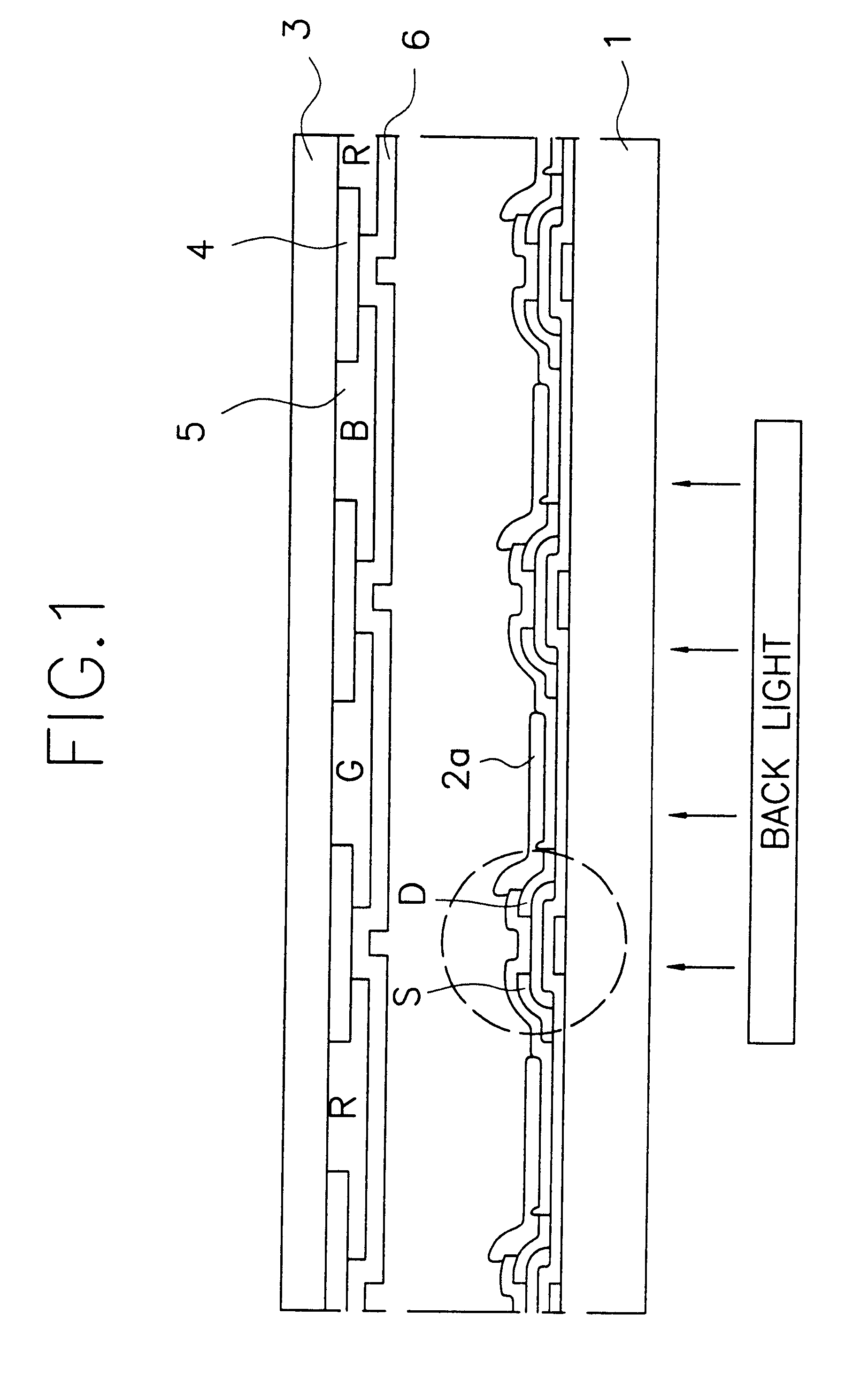
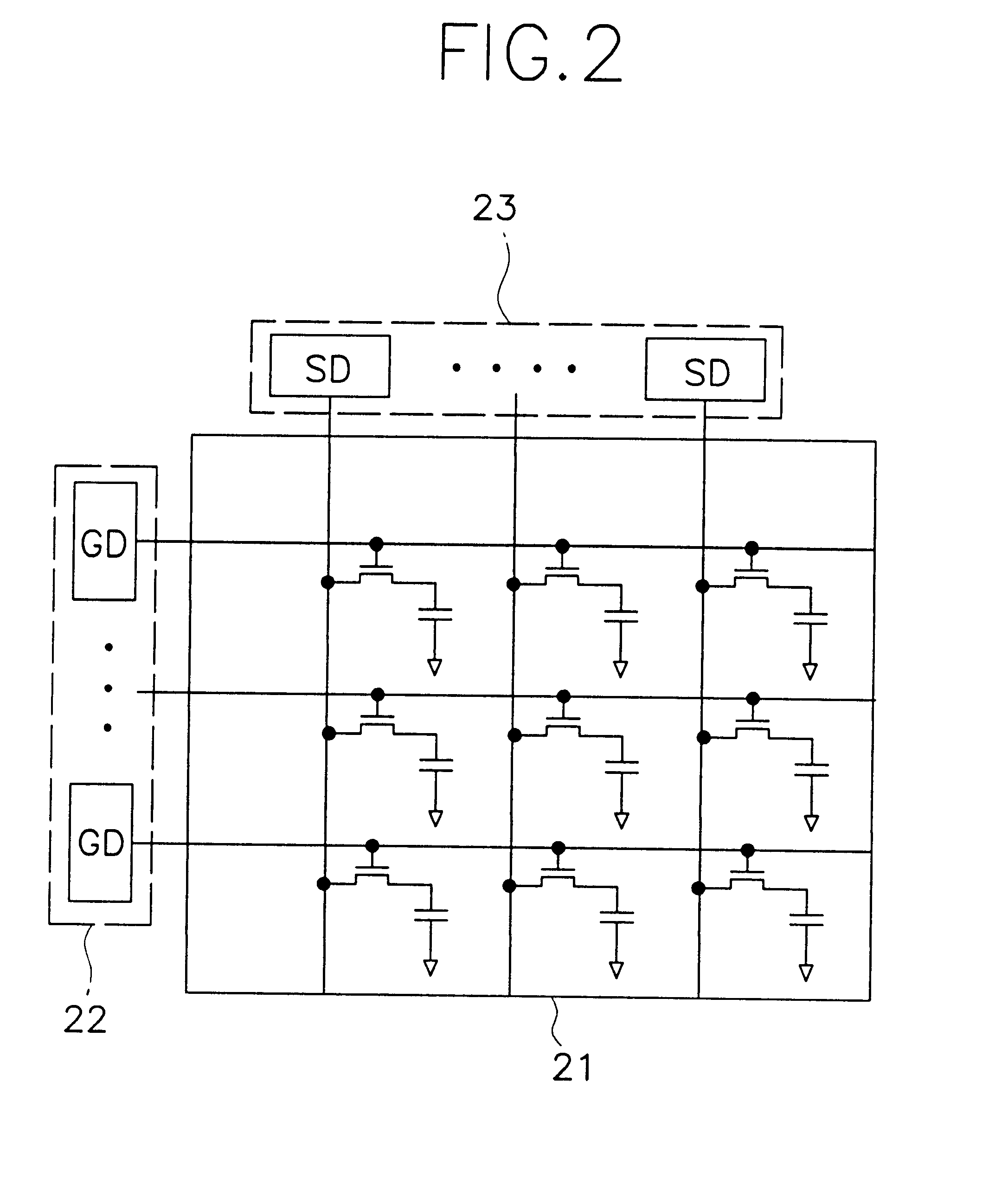
1. Field of the InventionThe present invention relates to a liquid crystal display and, more particularly, to a driver of liquid crystal display, in which the driving signal applied to the two scanning lines adjacent to each other is controlled to allow one data line to send two video signal to both pixels, respectively, thereby reducing the number of the data lines by half in comparison with the conventional liquid crystal display.2. Discussion of Related ArtA liquid crystal display generally consists of upper and lower plates and a liquid crystal being sealed between the two plates. The upper plate has a black matrix, a common electrode and R, G, and B color filter layers for displaying colors formed thereon. On the lower plate, data lines and gate lines are arranged, intersecting each other, to form pixel regions in matrix form. Each of the pixel regions includes one thin film transistor and one pixel electrode.FIG. 1 is a cross-sectional view of a general liquid crystal display....

Claims


Application Information

Patent Timeline
Patent Type & Authority Patents(United States)
IPC IPC(8): G09G3/36G09F9/30G02F1/133G09G3/20
CPCG09G3/3648G09G3/3659G09G3/3677G09G3/3688G09G3/3614G09G2310/06G09G2300/0814G09G2310/0251G09G2310/027G09G2310/0297G02F1/133
Inventor KWON, OH-KYONG
Owner SAMSUNG ELECTRONICS CO LTD
Why Eureka
Try Eureka