Integrated design system and method for reducing and avoiding crosstalk

a design system and integrated technology, applied in the field of avoiding noise in logic design, can solve problems such as chip failure, inability to correct logic responses, and inability to solve crosstalk problems, and achieve the effect of avoiding noise and reducing nois

Inactive Publication Date: 2003-07-15
BELL SEMICON LLC
View PDF8 Cites 73 Cited by
  • Summary
  • Abstract
  • Description
  • Claims
  • Application Information

AI Technical Summary

Problems solved by technology

Crosstalk can result in incorrect logic responses and, in the extreme, chip failure.
However, typically, these state of the art crosstalk analysis programs identify crosstalk errors only after circuit cell placement and wiring has been completed.
At this point in the design, once crosstalk problems are identified, correcting crosstalk problems may require significant effort, e.g., re-placing cells and rewiring circuits or re-buffering individual clocks and perhaps even redesigning the logic to split affected nodes.
Accordingly these prior approaches are time consuming and still may not lead to an acceptable chip design in a reasonable period of time.

Method used


Image

  • Integrated design system and method for reducing and avoiding crosstalk
  • Integrated design system and method for reducing and avoiding crosstalk
  • Integrated design system and method for reducing and avoiding crosstalk

Examples


Embodiment Construction

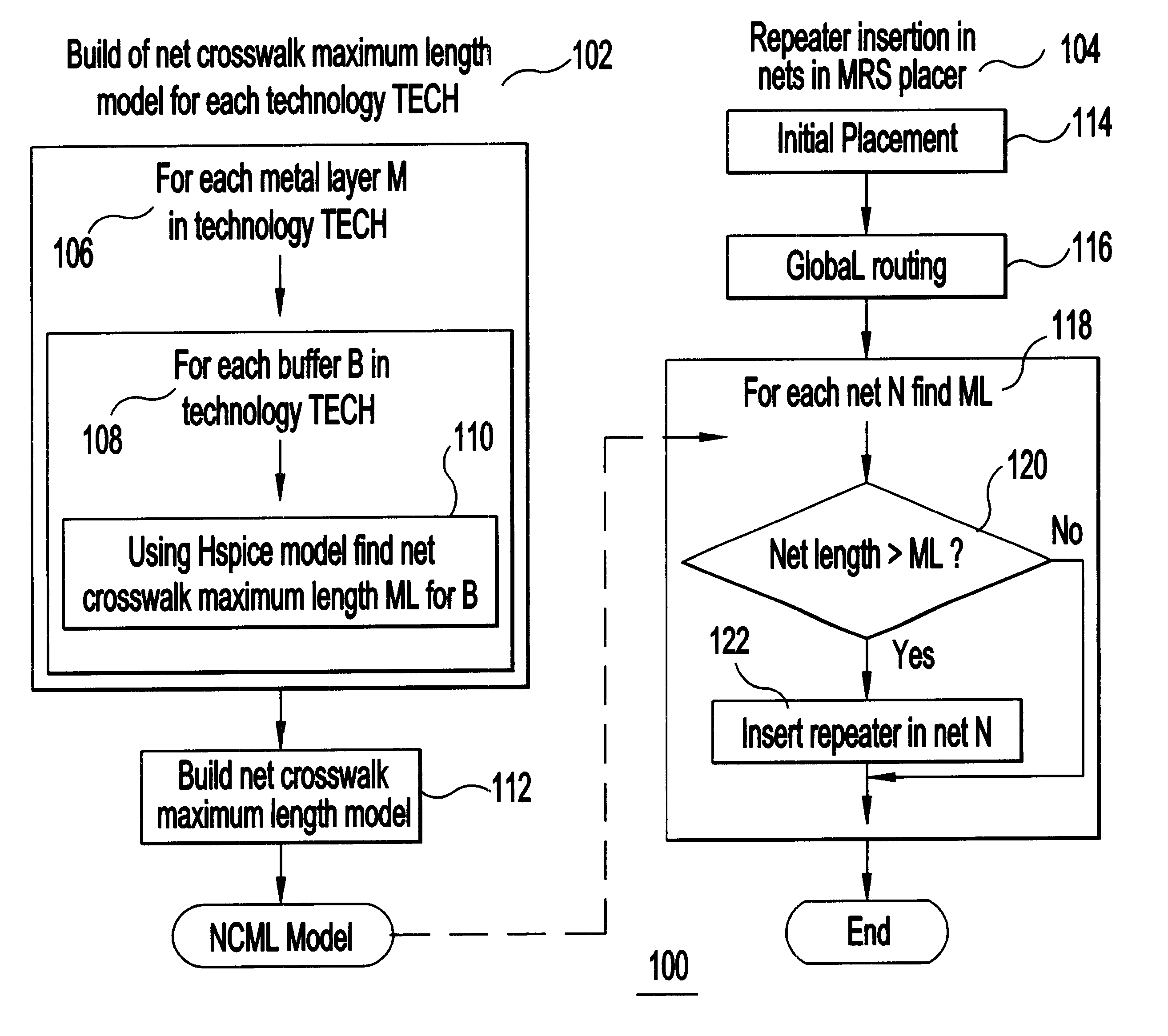
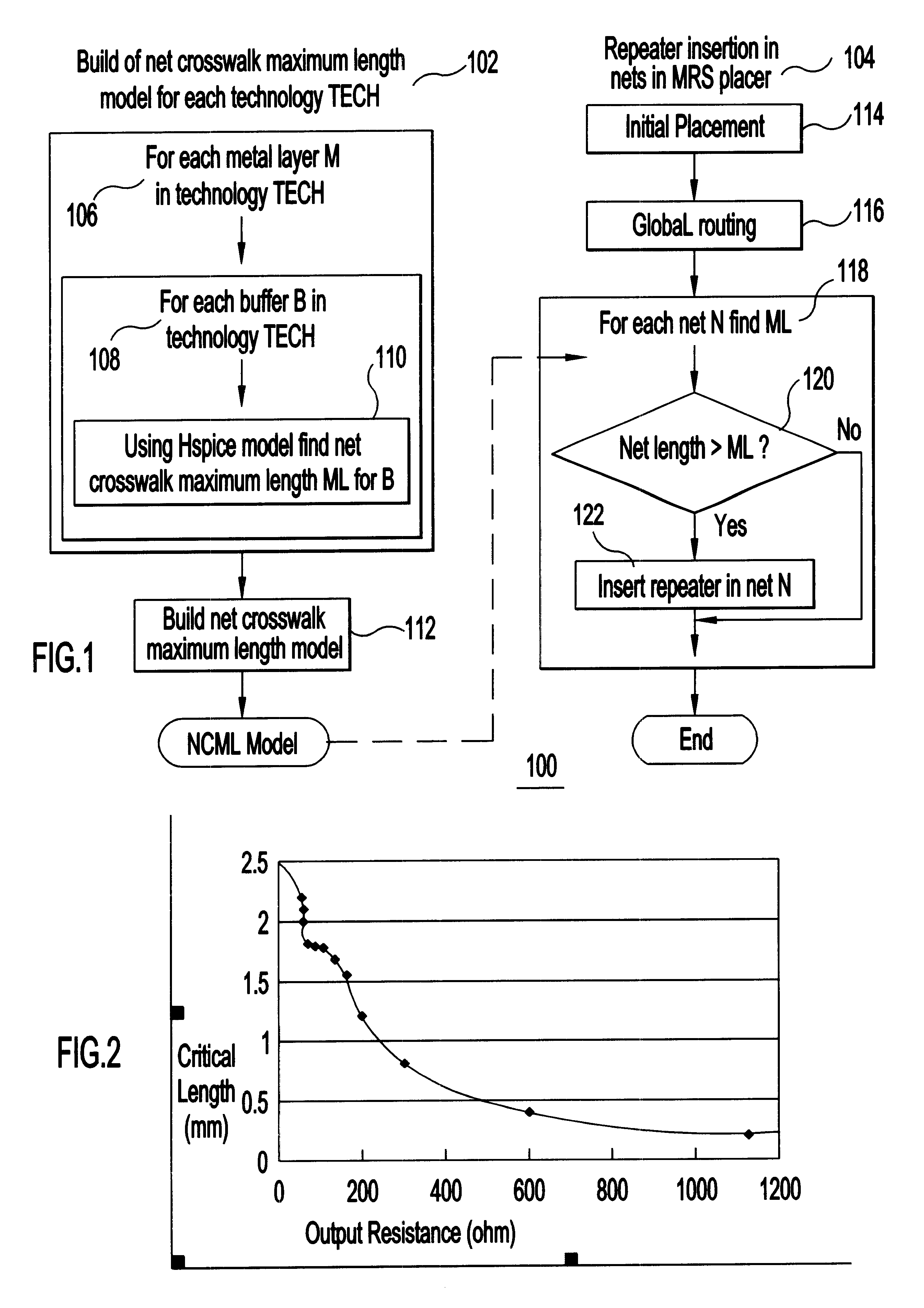
Turning now to the drawings and, more particularly, FIG. 1 is a flow diagram of an initial or coarse crosstalk reduction step 100 of the preferred embodiment of the present invention. This global crosstalk reduction step includes two major steps. The first major step 102 is a predesign phase or step, wherein wires are characterized for a particular technology to determine a critical length for wires at each layer. The second major step 104 is a segmentation step wherein, after placement, repeaters or buffers are inserted into any nets that have a total wire length greater than a technology defined critical length prior to cell wiring, thereby heading off any crosstalk that might otherwise occur.

So, first, a net crosstalk maximum length (NCML) model is generated in step 102 from existing designs. For each cell in each design a given crosstalk delay uncertainty (CDU) is assumed, e.g., 100 picoseconds (100 ps). The CDU is selected to be maintained within a specified design margin, for ...


PUM


Abstract

A system, method and program for hierarchically designing integrated circuits(ICs). Potential sources of crosstalk are identified in the hierachical design and prior to and during placement and wiring while maintaining the hierachical structure. Blocks are placed and analyzed to determine if all blocks are well behaved and where necessary selectively re-organized to be well behaved. Blockages are inserted blocks to restrict top level wiring to avoid crosstalk. Orthogonal restrictions are placed on top level wiring as well as on top level wire lengths.

Description

1. Field of the InventionThe present invention is related to noise avoidance in logic design and more particularly to reducing noise in integrated circuit logic chip designs.2. Background DescriptionNoise problems caused by cross coupling effects (crosstalk) from runs of parallel integrated circuit wires are well known in the art, especially for application specific integrated circuits (ASICs) designed in technologies based at 0.18 micrometers (microns) and below. Crosstalk can result in incorrect logic responses and, in the extreme, chip failure. Accordingly to identify potential crosstalk, circuit analysis tools such as GateScope.TM. from Moscape, Inc. have been developed.However, typically, these state of the art crosstalk analysis programs identify crosstalk errors only after circuit cell placement and wiring has been completed. At this point in the design, once crosstalk problems are identified, correcting crosstalk problems may require significant effort, e.g., re-placing cell...

Claims


Application Information

Patent Timeline
Patent Type & Authority Patents(United States)
IPC IPC(8): G06F17/50
CPCG06F17/5022G06F17/5036G06F17/5068G06F30/39G06F30/33G06F30/367G06F30/3308
Inventor TETELBAUM, ALEXANDERAL-DABAGH, MAAD A.HUANG, TAMMY T.
Owner BELL SEMICON LLC
Why Eureka
Try Eureka