Microelectronic package having a compliant layer with bumped protrusions

a microelectronic package and compliant technology, applied in the direction of semiconductor devices, semiconductor/solid-state device details, electrical equipment, etc., can solve the problems of complex microprocessor chips that may require many hundreds of connections to external devices, generally do not lend themselves to chips, and present serious drawbacks

Inactive Publication Date: 2005-01-25
TESSERA INC
View PDF32 Cites 137 Cited by
  • Summary
  • Abstract
  • Description
  • Claims
  • Application Information

AI Technical Summary

Benefits of technology

This patent describes how to make computer chips more efficiently compact while still ensuring their functionality. It achieves this through a design called "fan-in leads," which allows for minimal space usage when packaged. Additionally, it uses a special material (compliant layer) with rounded borders instead of sharp corners, which improves its stability during use. These technical improvements enhance the performance and durability of electronic devices made from these chips.

Problems solved by technology

The technical problem addressed in this patent text relates to improving the attachment of microelectronic components like semiconductor chips to circuit boards while also allowing them to thermally expand and contract without causing damage to the bonds connecting them. Current techniques involve wire bonding or tape automated bonding, but they often result in large assembled modules because of their fixed outer dimensions. Additionally, there is difficulty in testing the chips prior to attachment to ensure proper functionality and performance levels.

Method used


Image

  • Microelectronic package having a compliant layer with bumped protrusions
  • Microelectronic package having a compliant layer with bumped protrusions
  • Microelectronic package having a compliant layer with bumped protrusions

Examples


Embodiment Construction

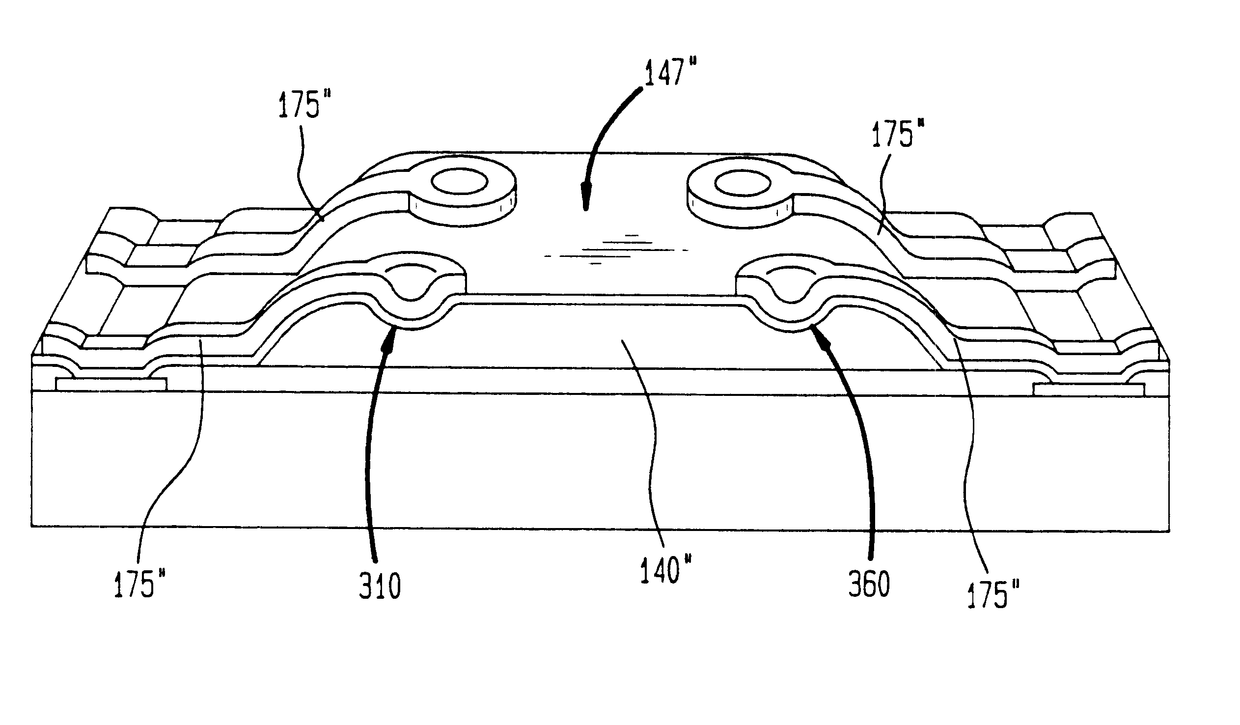
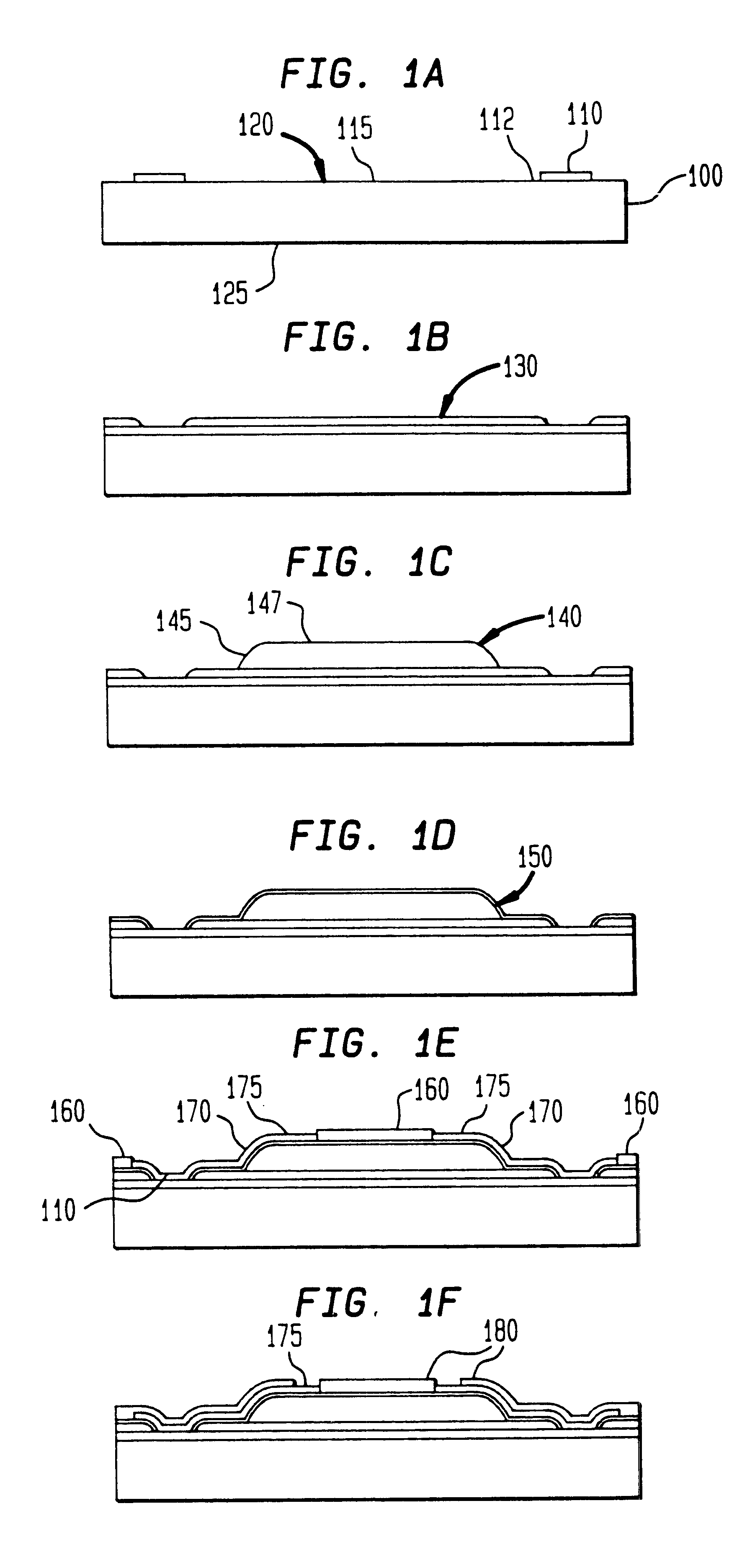
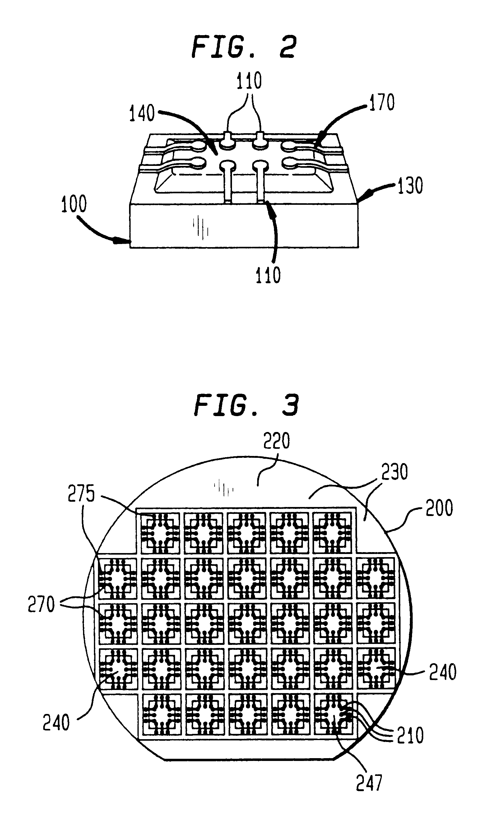
FIGS. 1A-F illustrate a side view of the process of creating the compliant chip package of the present invention on the face surface of a single die, on the face surfaces of multiple die arranged in a coplanar array or on the face surface of an undiced silicon wafer which may be subsequently diced into individual packaged chips or multi-chip modules.

FIG. 1A shows a single semiconductor chip 100 with a contact bearing face surface 120. The contacts 110 on the face surface 120 are typically aligned in a peripheral region 112 and further define a central region 115 therein. In FIG. 1B, a dielectric passivation layer is deposited or adhered onto the face surface 120 of the chip 100. The passivation layer may simply be the SiO2 passivation layer (not shown) commonly found on the contact bearing surface of semiconductor chips, or a separate dielectric passivation layer 130 may be used, such as an epoxy resin, a polyimide resin, photo-imagable dielectric, etc. If the separate passivation l...


PUM


Abstract

A microelectronic assembly includes a microelectronic element having a first surface with a plurality of contacts accessible at the first surface, and a compliant layer over the first surface of the microelectronic element, the compliant layer including a plurality of bumped protrusions and openings adjacent the bumped protrusions for providing access to the contacts, wherein each bumped protrusion includes a top surface and at least one sloping edge. The microelectronic assembly also includes conductive terminals over the top surfaces of the bumped protrusions, and a plurality of conductive bond ribbons having first ends in engagement with the contacts, second ends in engagement with the terminals and intermediate sections extending along the sloping edges for electrically interconnecting the contacts and the terminals.

Description


Claims


Application Information

Patent Timeline
Owner TESSERA INC
Why Eureka
Try Eureka