Semiconductor device and method for fabricating the same

Active Publication Date: 2006-03-16
DONGBU ELECTRONICS CO LTD +1
View PDF2 Cites 0 Cited by
  • Summary
  • Abstract
  • Description
  • Claims
  • Application Information

AI Technical Summary

Benefits of technology

[0016] The present invention minimi

Problems solved by technology

In the aforementioned method, the process for exposing the electrode pad to the external power source is very complicated.
Also, when exposing the electrode pad, the electrode pad may be corroded due to chemicals, whic

Method used


Image

  • Semiconductor device and method for fabricating the same
  • Semiconductor device and method for fabricating the same
  • Semiconductor device and method for fabricating the same

Examples


Embodiment Construction

[0028] Reference will now be made in detail to exemplary embodiments of the present invention which are illustrated in the accompanying drawings. Wherever possible, the same reference numbers will be used throughout the drawings to refer to the same or like parts.

[0029] Hereinafter, a semiconductor device and a method for fabricating the same according to the present invention will be described as follows.

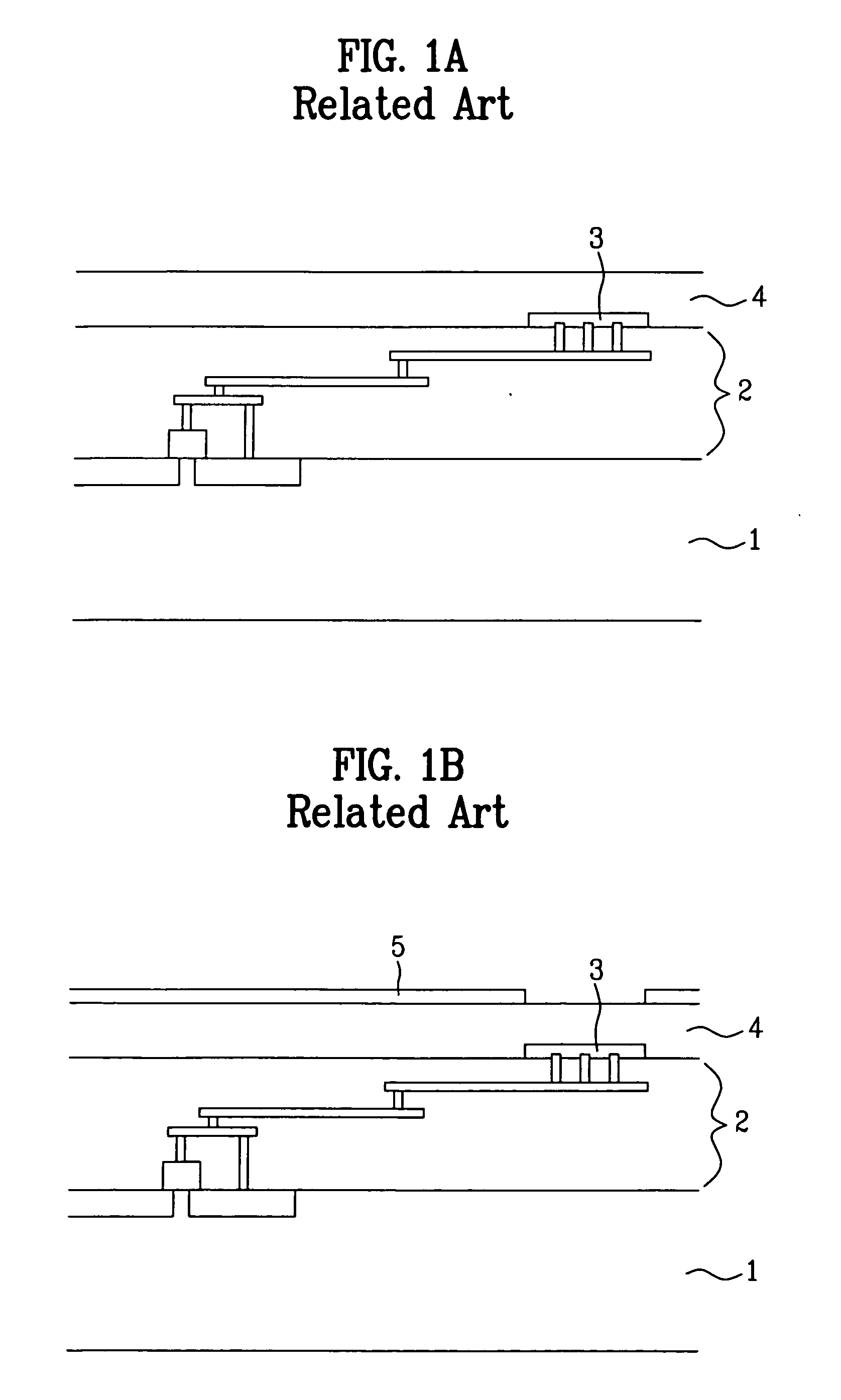
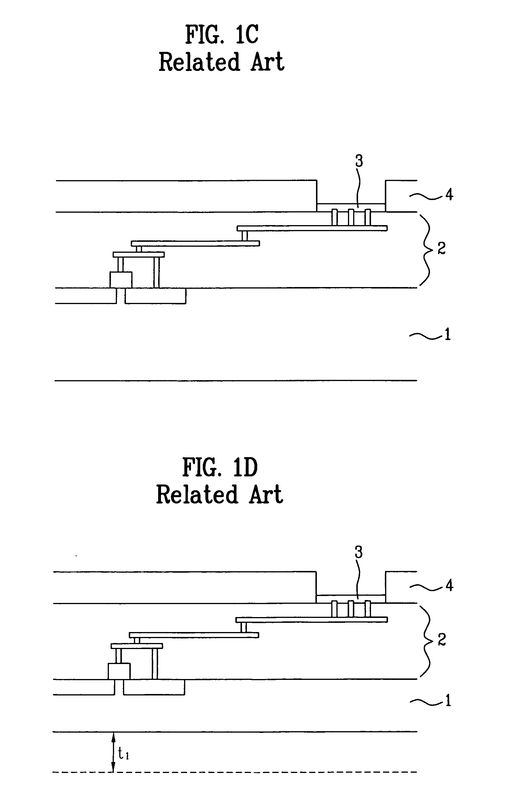
[0030] A fabrication method of a semiconductor device includes a fabrication process for forming a circuit device by forming a minute pattern in a silicon wafer, a packaging process for providing electricity to individual chips of the silicon wafer of the circuit device, and sawing and packaging the individual chips. In the present invention, the fabrication process is simplified by simplifying an electrode pad formation process. The size of product is minimized after the packaging process.

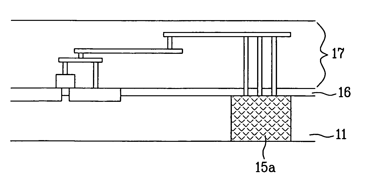
[0031]FIG. 2G is a cross sectional view of a semiconductor device according to one preferr...


PUM


Abstract

A method for fabricating a semiconductor device including forming a depression in a front surface of a semiconductor substrate, forming an electrode pad within the depression, forming structures including circuit devices and metal wires on the front surface of the semiconductor substrate, and exposing the electrode pad by removing a rear surface of the semiconductor substrate.

Description

BACKGROUND OF THE INVENTION [0001] 1. Field of the Invention [0002] The present invention relates to a method for fabricating a semiconductor device, and more particularly, to a semiconductor device and a method for fabricating the same minimizing the size of a product after a packaging process. [0003] 2. Discussion of the Related Art [0004] Generally, a method for fabricating a semiconductor device includes a fabrication process for forming a plurality of chips. A conventional process typically includes forming each chip with a circuit device by forming a minute pattern on a silicon wafer, a packaging process for providing electricity to individual chips of the silicon wafer, and sawing and packaging the individual chips. [0005] In the fabrication process for the semiconductor device, after the circuit device designed with various metals is formed on the silicon wafer, a nitride layer or an oxide layer is coated thereon so as to protect the chips. The nitride or oxide layer protect...

Claims


Application Information

Patent Timeline
IPC IPC(8): H01L29/40
CPCH01L21/76898H01L23/481H01L2224/48463H01L2924/01013H01L2924/01079H01L2924/10253H01L24/48H01L2924/00014H01L2924/00H01L24/45H01L2224/451H01L2924/00015H01L21/768H01L21/60
Inventor JUNG, MENG AN
Owner DONGBU ELECTRONICS CO LTD
Why Eureka
Try Eureka