

Chip package structure having function of preventing adhesive from overflowing
a chip and packaging technology, applied in the field of packaging technology, can solve the problems of difficulty in applying the higher viscosity glue to the carrier board, conventional chip package structure still has drawbacks, and therefore needs improvement, and achieve the effect of reducing the size of the chip package structur
- Summary
- Abstract
- Description
- Claims
- Application Information
AI Technical Summary
Benefits of technology
Problems solved by technology
Method used
Image

Examples
Embodiment Construction
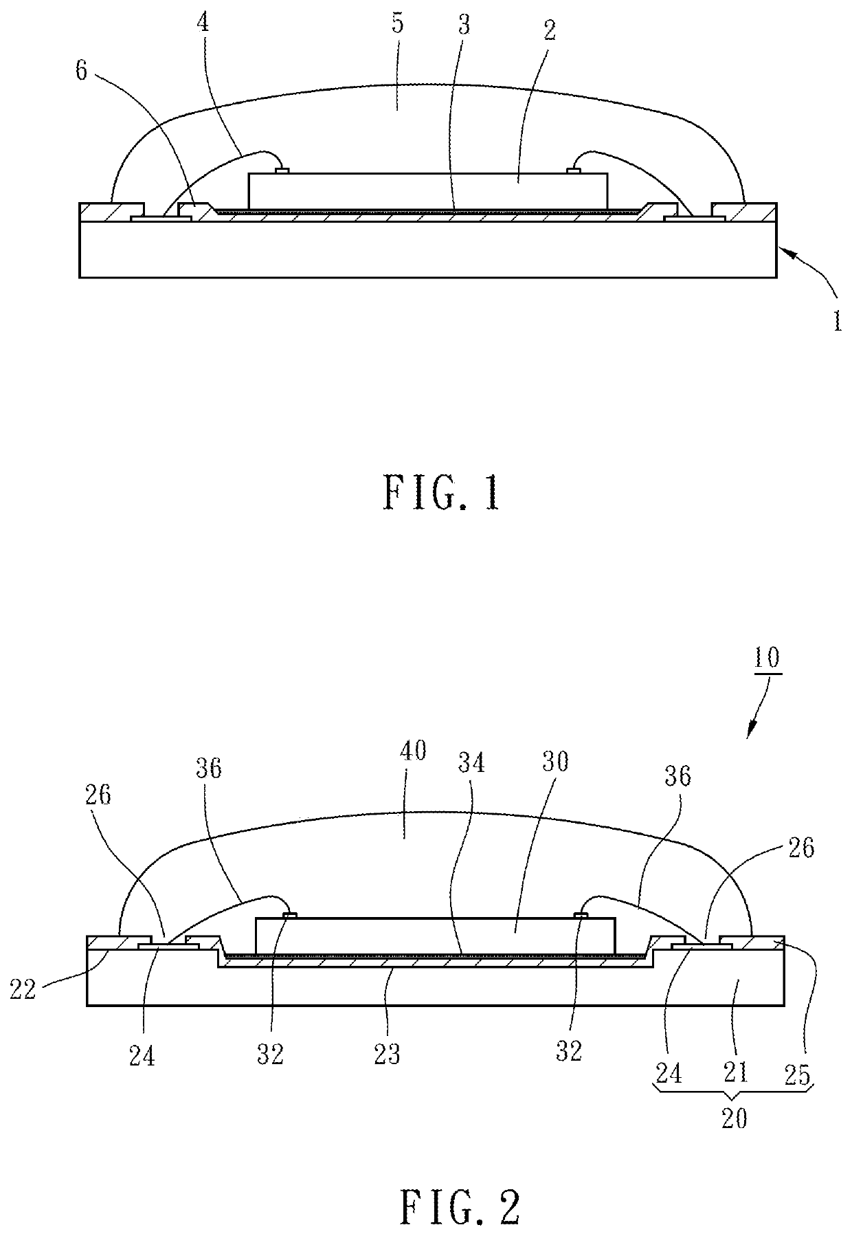
[0010]Referring to FIG. 2, a chip package structure 10 of the present invention includes a carrier board 20, a chip 30, and a package glue 40.
[0011]The carrier board 20 has a substrate 21, an unlimited number of first conductive pads 24, and a solder mask 25. The substrate 21 is provided with an upper surface 22 and a concavity 23 formed on the upper surface 22 and having a depth greater than 0.1 mm. The first conductive pads 24 are mounted on the upper surface 22 of the substrate 21 and arranged around the concavity 23 of the substrate 21. The solder mask 25 is applied to the substrate 21 and provided with a plurality of openings 26, wherein each of the openings 26 exposes a portion of one of the first conductive pads 24. Further, the substrate 21 in the present embodiment may, but unlimited to, be a bismaleimide-triazine (usually referred to as “BT”) substrate, a glass fiber substrate (usually referred to as “FR4”), or a direct bonded copper (usually referred to as “DBC”) substrat...
PUM
| Property | Measurement | Unit |
|---|---|---|
| depth | aaaaa | aaaaa |
| conductive | aaaaa | aaaaa |
| area | aaaaa | aaaaa |
Abstract
Description
Claims
Application Information