Electroetching process and system

a technology of electroetching and process, applied in the direction of basic electric elements, electrical equipment, semiconductor/solid-state device manufacturing, etc., can solve the problems of removing conductive materials off the wafer surface, which is known to be quite expensive, and achieves the effect of reducing the cost of removal

Inactive Publication Date: 2005-02-08
NOVELLUS SYSTEMS
View PDF5 Cites 73 Cited by
  • Summary
  • Abstract
  • Description
  • Claims
  • Application Information

AI Technical Summary

Problems solved by technology

These removal processes are known to be quite costly.
However, in such processes there are problems in removing conductive materials off the wafer surface uniformly and in a controllable manner.

Method used


Image

  • Electroetching process and system
  • Electroetching process and system
  • Electroetching process and system

Examples


Embodiment Construction

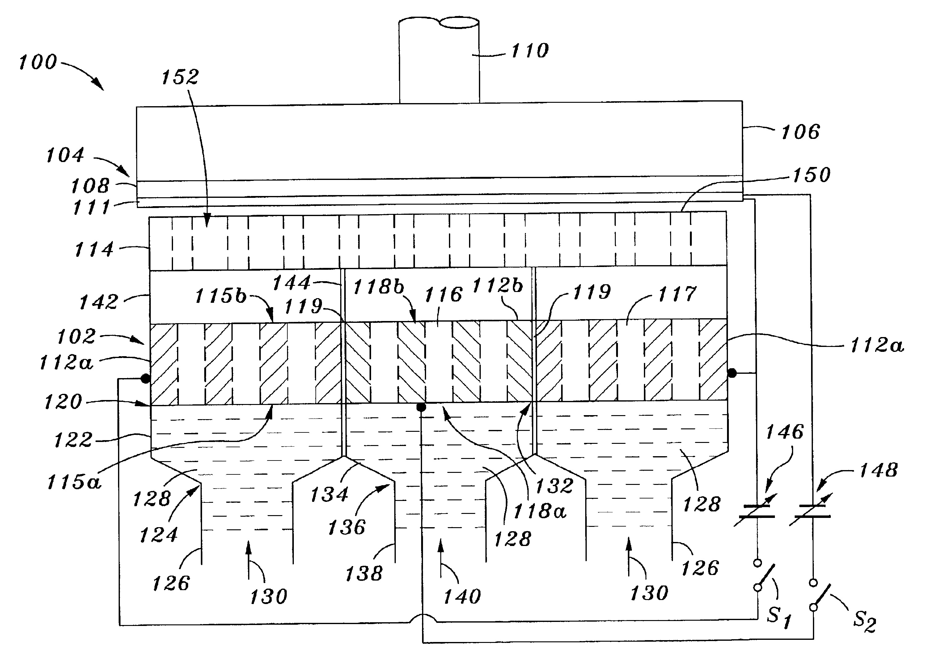
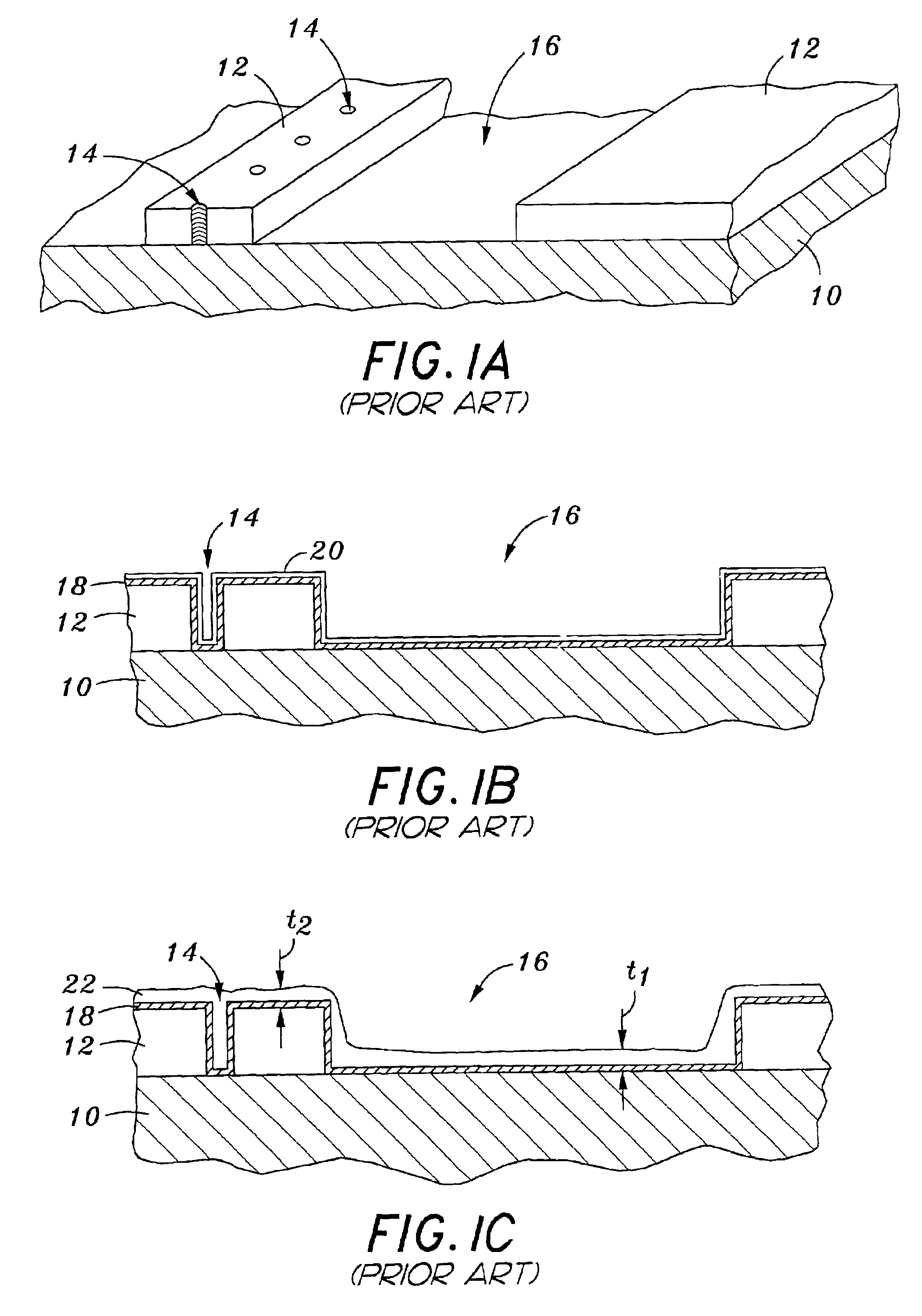
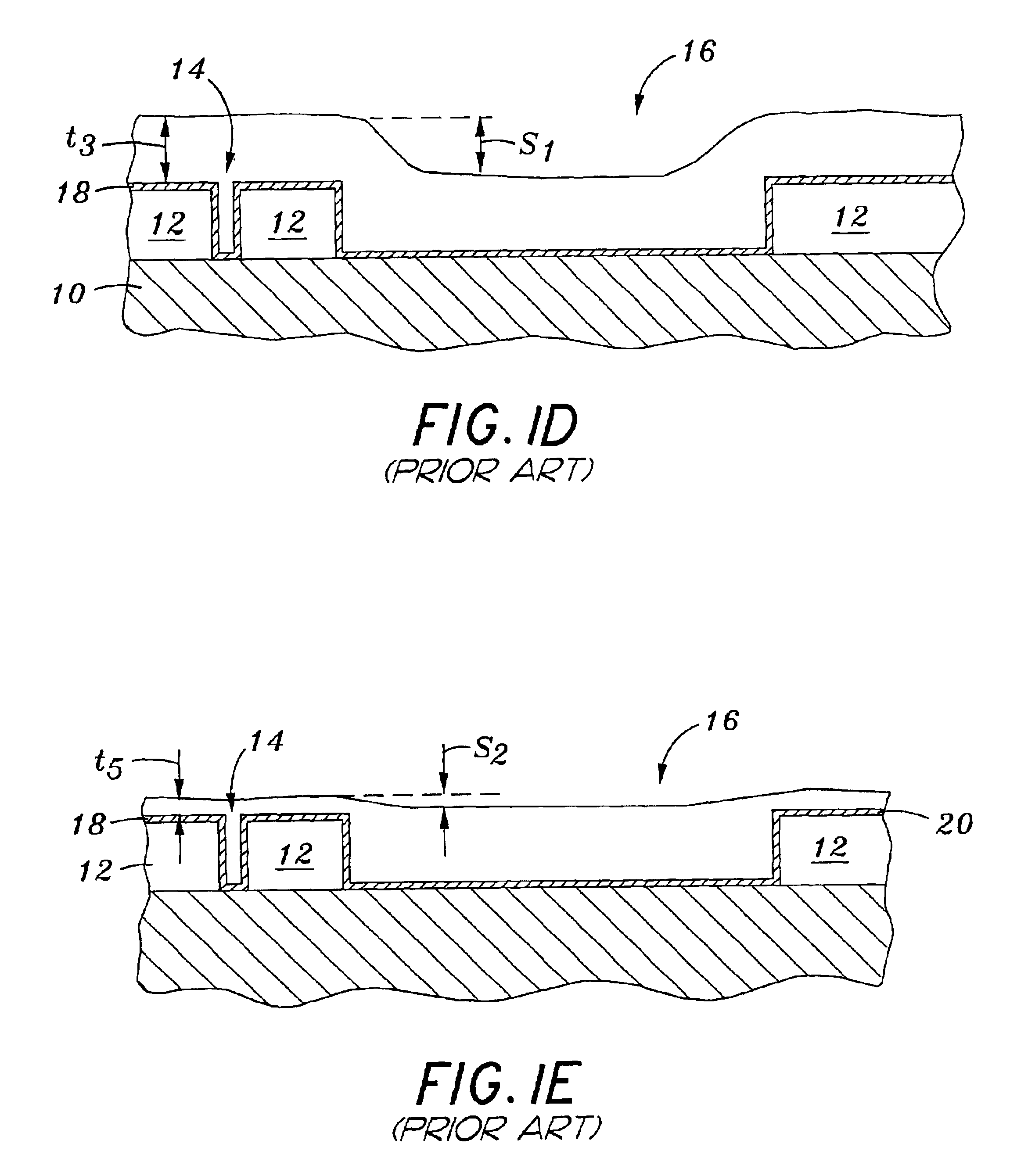
As will be described below, the present invention provides a method and a system to selectively electrochemically remove a conductive material layer deposited on a surface of a semiconductor. The invention can be used with ECMD, other plating systems that yield planar deposits, as well as other plating systems that deposit conformal films. In general, when a conductive surface of substrate or work piece is electroetched or electropolished some regions on the conductive surface may be etched faster than the other regions of the conductive surface. For example, during an electroetching process of a surface of a wafer, the current density applied to the surface is substantially greater at the periphery of the surface than the center of the surface. In the prior art, this higher current density results in an increased etching rate of the deposited film at the periphery of the wafer as compared to the wafer center. With the present invention, the etching difference between the interior a...


PUM

PropertyMeasurementUnit
aspect ratioaaaaaaaaaa
conductiveaaaaaaaaaa
poweraaaaaaaaaa

Abstract

A system for optionally depositing or etching a layer of a wafer includes mask plate opposed to the wafer with the mask plate having a plurality of openings that transport a solution to the wafer. An electrode assembly has a first electrode member and a second electrode member having channels that operatively interface a peripheral and center part of the wafer. The channels transport the solution to the mask.

Description

FIELD OF THE INVENTIONThe present invention generally relates to electroetching process technology and, more particularly, to an electroetching process and apparatus to yield planar deposition layers.BACKGROUND OF THE INVENTIONConventional semiconductor devices generally include a semiconductor substrate, usually a silicon substrate, and a plurality of sequentially formed dielectric interlayers such as silicon dioxide and conductive paths or interconnects made of conductive materials. The interconnects are usually formed by filling a conductive material in trenches etched into the dielectric interlayers. In an integrated circuit, multiple levels of interconnect networks laterally extend with respect to the substrate surface. The interconnects formed in different layers can be electrically connected using vias or contacts. A conductive material filling process of such features, i.e., via openings, trenches, pads or contacts, can be carried out by depositing a conductive material over...

Claims


Application Information

Patent Timeline
Patent Type & Authority Patents(United States)
IPC IPC(8): C25F3/14C25F3/00H01L21/70H01L21/02H01L21/288H01L21/321H01L21/768H01L21/3213B23H5/08
CPCB23H5/08C25F3/14H01L21/7684H01L21/32115H01L21/32134H01L21/2885
Inventor BASOL, BULENT M.UZOH, CYPRIANYAKUPOGLU, HALIT N.TALIEH, HOMAYOUN
Owner NOVELLUS SYSTEMS
Why Eureka
Try Eureka