FinFET gate formation using reverse trim and oxide polish

a reverse trim and oxide polish technology, applied in the field of transistors, can solve the problems of limited difficult, if not impossible, scaling of existing bulk mosfet devices below the 0.1 m process generation, etc., and achieves wide photo margin, wide photo margin, and increased printing and patterning ability.

Inactive Publication Date: 2005-02-15
INNOVATIVE FOUNDRY TECH LLC
View PDF21 Cites 74 Cited by
  • Summary
  • Abstract
  • Description
  • Claims
  • Application Information

AI Technical Summary

Benefits of technology

Consistent with the present invention, a method of forming a gate of a FinFET transistor is provided that permits a wide photo margin. Consistent with the invention, a reverse trim process may be employed for forming a gate within a layer of material, such as, for example, an oxide layer. The gate may be formed within the oxide layer by applying a photo-resist material in a pattern, corresponding to a shape of the gate, to the oxide layer. A layer of the oxide layer may then be etched away to produce a raised portion of the oxide layer in the shape of the pattern of the photo-resist material. A nitride layer may then be applied to the exposed surface of the oxide layer. The nitride layer, formed on the raised portion of the oxide layer, and the upper part of the raised portion of the oxide layer may be polished off to expose a portion of the oxide layer in the shape of the pattern of the photo-resist material. The exposed oxide may be etched, selective to nitride and the material of the fin, to create a trench that is approximately transverse to the underlying fin. The gate electrode may be then formed within the created trench. Formation of the gate electrode, consistent with the invention, permits a wide photo margin, thus, increasing the ability to print and pattern the small features of the FinFET gate.

Problems solved by technology

Due to limitations associated with existing gate-oxide thicknesses and source / drain (S / D) junction depths, scaling of existing bulk MOSFET devices below the 0.1 μm process generation may be difficult, if not impossible.
The severe topography associated with the FinFET structure has conventionally limited the ability to print and pattern small features for the FinFET gate.

Method used


Image

  • FinFET gate formation using reverse trim and oxide polish
  • FinFET gate formation using reverse trim and oxide polish
  • FinFET gate formation using reverse trim and oxide polish

Examples


Embodiment Construction

The following detailed description of the invention refers to the accompanying drawings. The same reference numbers in different drawings may identify the same or similar elements. Also, the following detailed description does not limit the invention. Instead, the scope of the invention is defined by the appended claims.

Consistent with the present invention, a reverse trim process for creating FinFET gates is provided that increases the ability to print and pattern small features of the FinFET gate. The reverse trim process enables formation of trimmed damascene gates that allow wide photo margins.

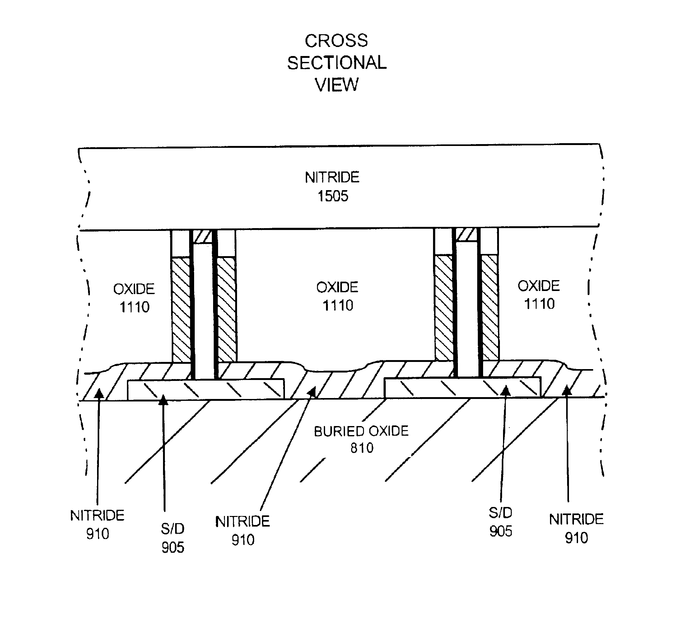
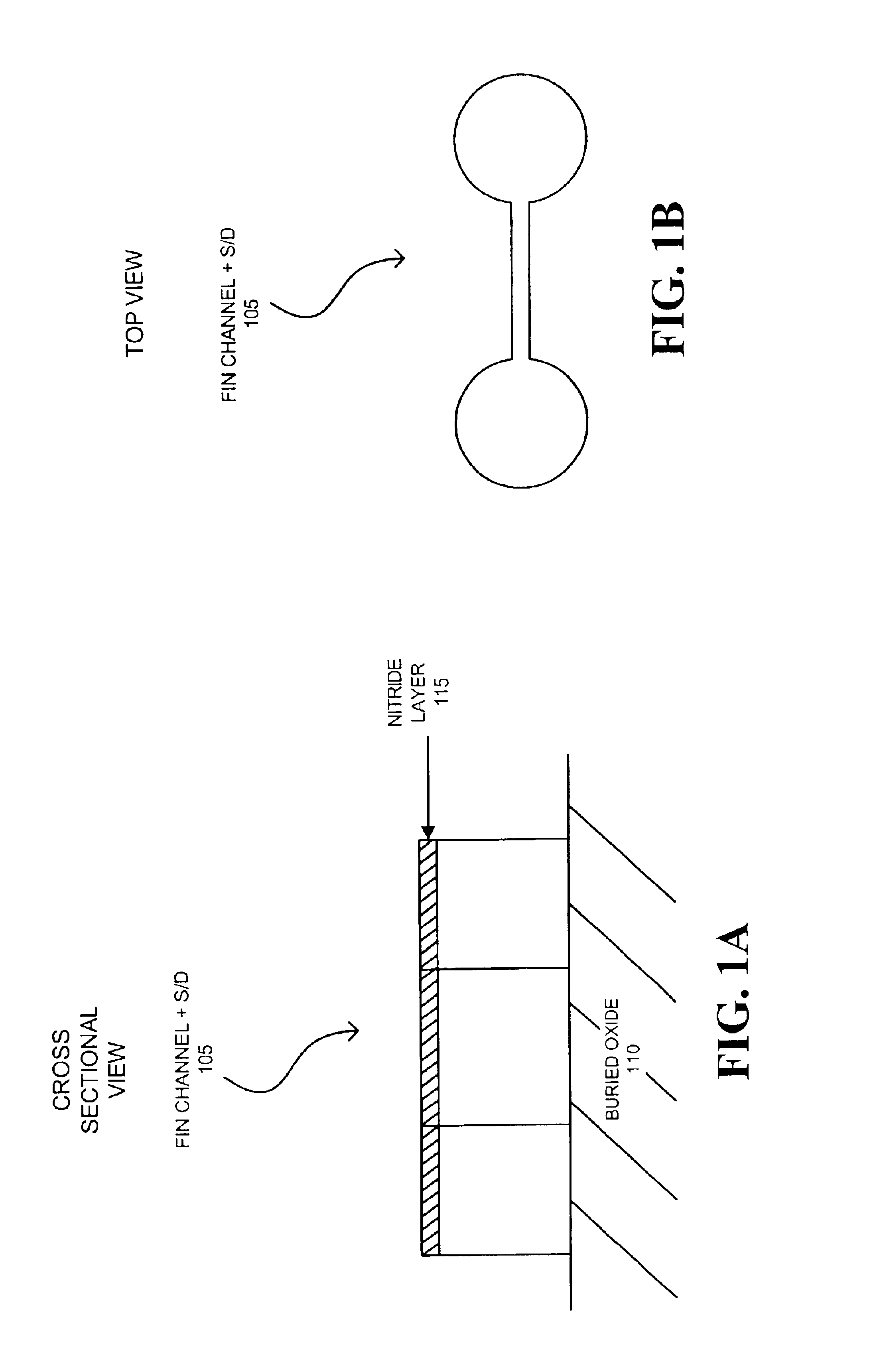
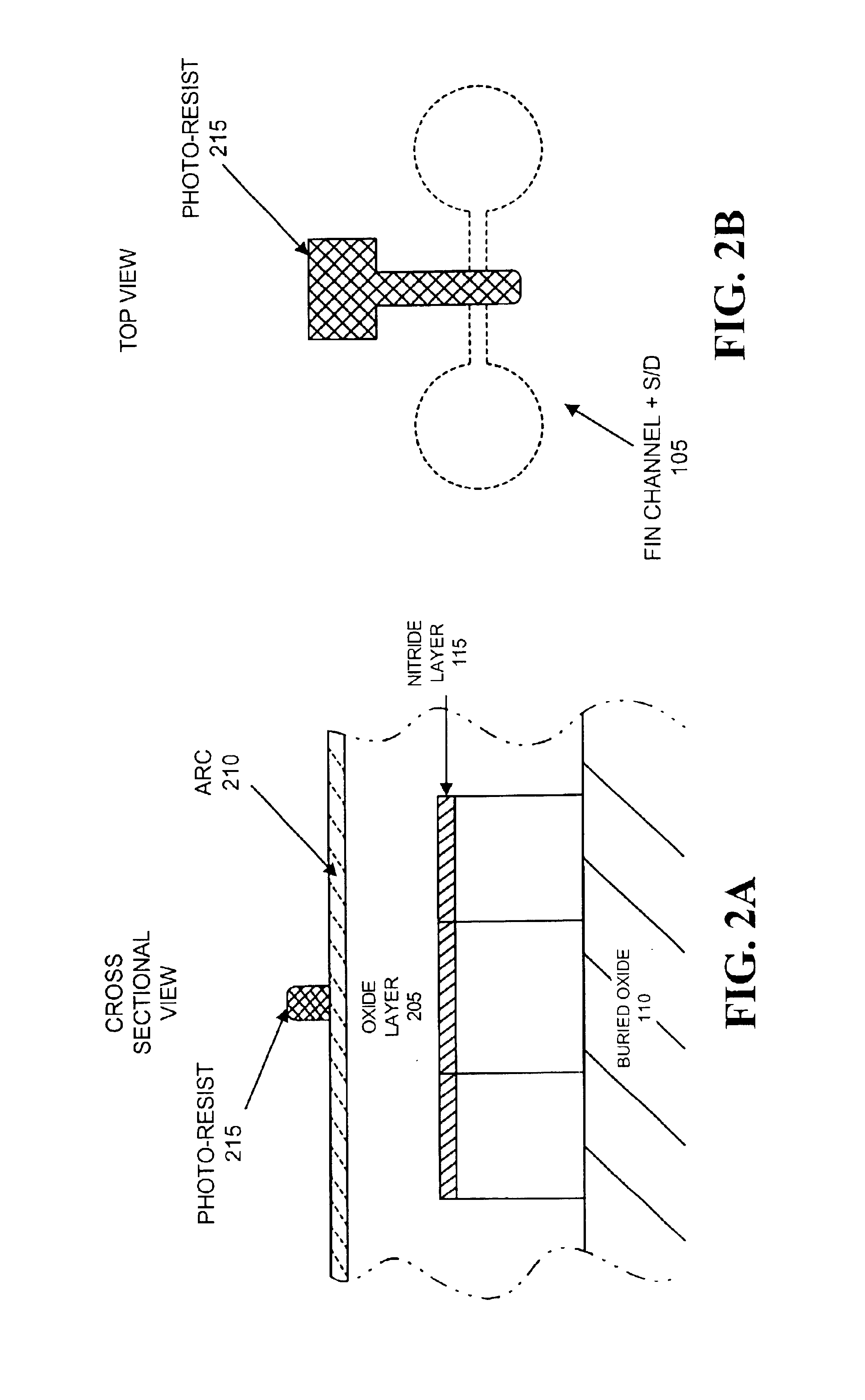
FIGS. 1A and 1B illustrate a FinFET fin channel and source / drain (S / D) 105 formed on a buried oxide layer 110 in accordance with an exemplary embodiment of the present invention. Fin channel and S / D 105 maybe formed on buried oxide layer 110 using any conventional technique. Fin channel and S / D 105 may include, for example, silicon (Si). Other materials, such as Germanium (Ge), may alterna...


PUM


Abstract

A method of forming a gate electrode for a fin field effect transistor (FinFET) is provided. The method includes forming a fin on a substrate and forming an oxide layer over the fin. The method further includes forming a trench in the oxide layer, the trench crossing over the fin, and filling the trench with a material to form a gate electrode.

Description

TECHNICAL FIELDThe present invention relates generally to transistors and, more particularly, to fin field effect transistors (FinFETs).BACKGROUND ARTScaling of device dimensions has been a primary factor driving improvements in integrated circuit performance and reduction in integrated circuit cost. Due to limitations associated with existing gate-oxide thicknesses and source / drain (S / D) junction depths, scaling of existing bulk MOSFET devices below the 0.1 μm process generation may be difficult, if not impossible. New device structures and new materials, thus, are likely to be needed to improve FET performance.Double-gate MOSFETs represent new devices that are candidates for succeeding existing planar MOSFETs. In double-gate MOSFETs, the use of two gates to control the channel significantly suppresses short-channel effects. A FinFET is one example of a recent double-gate structure that includes a channel formed in a vertical fin. The FinFET is similar to existing planar MOSFETS in...

Claims


Application Information

Patent Timeline
Patent Type & Authority Patents(United States)
IPC IPC(8): H01L21/00H01L21/336H01L29/786
CPCH01L29/42392H01L29/78642H01L29/785H01L29/66818
Inventor DAKSHINA-MURTHY, SRIKANTESWARATABERY, CYRUS E.
Owner INNOVATIVE FOUNDRY TECH LLC
Why Eureka
Try Eureka