Scanning probe microscopy inspection and modification system

a microscopy and scanning probe technology, applied in the direction of electrostatic motors, electrical/magnetic measuring arrangements, record information storage, etc., can solve problems such as the defectiveness of the prob

Inactive Publication Date: 2005-03-01
TERRASPAN
View PDF40 Cites 50 Cited by
  • Summary
  • Abstract
  • Description
  • Claims
  • Application Information

AI Technical Summary

Benefits of technology

The generated inspection data is then compared with target data (or parameters). This target data may include a target image and/or analysis of the object which is/are compared with the generated image and/or analysis. If they do not match within a predefined tolerance level, then modification data is generated that identifies the types of modifications that need to be made to the object to fall within the tolerance level. These modifications may be simply to remove particle contaminants on the object or more importantly to structurally and/or chemically modif

Problems solved by technology

A probe may be defective because of w

Method used


Image

  • Scanning probe microscopy inspection and modification system
  • Scanning probe microscopy inspection and modification system
  • Scanning probe microscopy inspection and modification system

Examples


Embodiment Construction

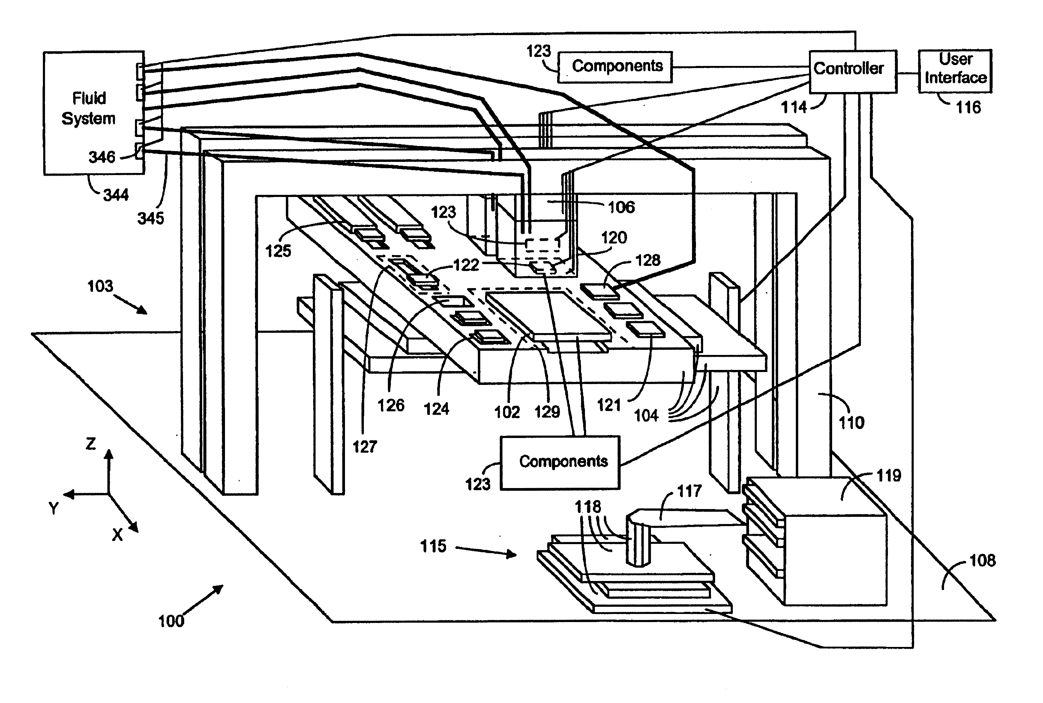
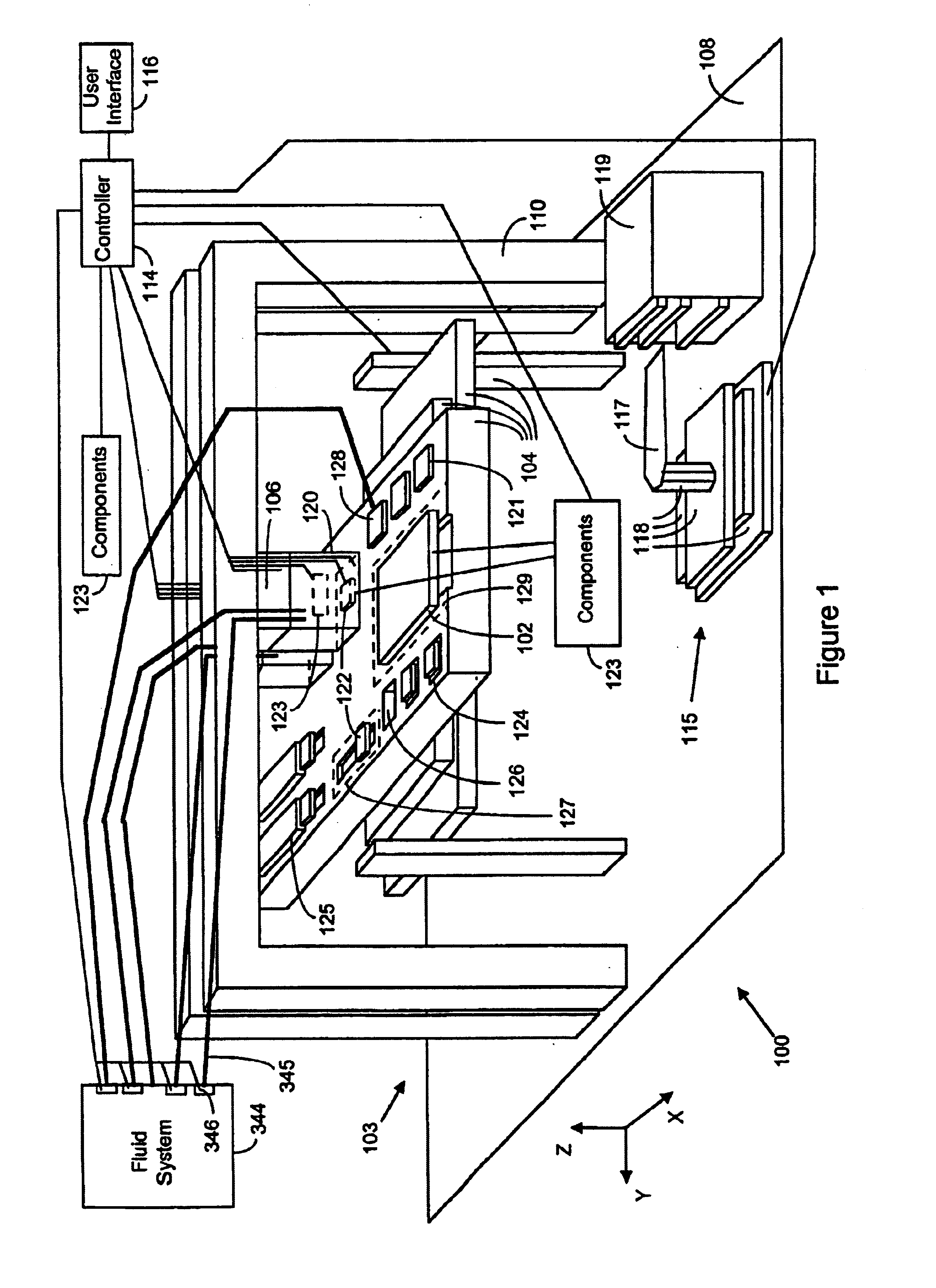
Referring to FIG. 1, there is shown an exemplary embodiment of an SPM (scanning probe microscopy) object inspection and / or modification system 100 which uses SPM technology and techniques in new and novel ways to inspect and / or modify an object 102. For example, as will be discussed throughout this document, the system can be used to perform tests, fabrication (i.e., manufacturing) steps, and / or repairs on semiconductor wafers and fabrication masks, lithographic structures (i.e., masters), and thin film magnetic read / write heads. Additionally, as will also be discussed throughout this document, the SPM system can also be used to analyze and / or alter biological or chemical samples.

The components of the SPM system 100 include a positioning system 103 that comprises a rough positioning apparatus 104, fine positioning apparatuses 106, a support table 108, and scanning head support structures 110. The rough positioning apparatus comprises a rough 3-D (i.e., three dimensions) translator, ...


PUM


Abstract

A scanning probe microscopy (SPM) inspection and/or modification system which uses SPM technology and techniques. The system includes various types of microstructured SPM probes for inspection and/or modification of the object. The components of the SPM system include microstructured calibration structures. A probe may be defective because of wear or because of fabrication errors. Various types of reference measurements of the calibration structure are made with the probe or vice versa to calibrate it. The components of the SPM system further include one or more tip machining structures. At these structures, material of the tips of the SPM probes may be machined by abrasively lapping and chemically lapping the material of the tip with the tip machining structures.

Description

FIELD OF THE INVENTIONThe present invention relates generally to systems and methods for modifying and / or inspecting an object. In particular, it pertains to a system and method for using nanostructured and nanopositioned probes to remove material from or add material to an object, chemically change the material of an object, and / or analyze the material of an object.BACKGROUND OF THE INVENTIONCommon microfabrication techniques such as e-beam, laser beam, and standard photolithography are used to directly make or modify semiconductor wafers or fabrication masks. However, these techniques suffer from limitations in the size and energy which may to be used to create, modify, and inspect structures on the wafers or masks. Specifically, it is desirable that techniques be available to create, modify, and inspect structures in the range of a single molecule (approximately 1 Angstrom or less). However, the current techniques are unable to create, modify, and inspect structures at and below ...

Claims


Application Information

Patent Timeline
IPC IPC(8): G02B21/00G03F7/20G03F1/00G12B21/06G12B21/20G12B21/08G12B21/02G12B21/00G12B21/04G11B5/23G11B5/31G01B7/31G01B7/34G01Q10/00G01Q10/02G01Q10/04G01Q20/00G01Q20/02G01Q30/00G01Q30/02G01Q40/00G01Q40/02G01Q60/04G01Q60/10G01Q60/18G01Q60/24G01Q60/58G01Q70/02G01Q70/16G01Q80/00G03F1/72G03F1/84G11B5/00G11B9/00G11B11/12G11B11/16H02N1/00
CPCG11B9/14G11B9/1409G11B9/1418G11B9/1427G11B9/1436G11B9/1445G11B9/1454G11B9/149H02N1/006B82Y10/00B82Y20/00B82Y35/00G01B7/31G01N23/225G01Q10/02G01Q10/04G01Q10/06G01Q20/00G01Q20/02G01Q30/04G01Q40/00G01Q60/04G01Q60/58G01Q70/02G01Q70/06G02B21/002G03F1/72G03F1/84G03F7/2049G03F7/704G03F7/70616G01Q60/16G01Q60/22G01Q60/38G11B5/3116Y10S977/855G11B5/3166G11B11/12G11B11/16G11B2005/0002G11B2005/0021G01Q80/00G11B5/232Y10S977/871G11B5/3163
Inventor KLEY, VICTOR B.
Owner TERRASPAN
Why Eureka
Try Eureka