Zero-crossing direction and time interval jitter measurement apparatus using offset sampling

a technology of offset sampling and zero-crossing direction, applied in the field of test and measurement system, can solve the problems of insufficient bandwidth of real-time digital oscilloscope to faithfully digitize 40 gb, trade-offs between jitter transfer bandwidth and real-time digital oscilloscope, etc., to eliminate trigger circuit jitter, accurate extrapolate the zero-crossing time value, eliminate the effect of jitter

Inactive Publication Date: 2005-03-08
AGILENT TECH INC
View PDF11 Cites 25 Cited by
  • Summary
  • Abstract
  • Description
  • Claims
  • Application Information

AI Technical Summary

Benefits of technology

Advantageously, offset sampling of the signal-under-test allows the direction (up or down) of a signal zero-crossing to be ascertained without prior knowledge of the direction, as well as to accurately extrapolate the zero-crossing time value. In addition, adjusting the offset between the two samples to an integer multiple of the bit period of the signal under test enables both sampling of adjacent zero-crossings spaced from one to many bit intervals apart and a determination of the time interval jitter between adjacent zero-crossings. Moreover, offset sampling using a single trigger circuit eliminates the trigger circuit jitter from the time interval jitter analysis. Likewise, when using multiple sampling strobes, offset reference clock sampling eliminates the jitter related to the sampling strobe and sampling event. As a further advantage, the sampling apparatus of the present invention applies to all optical, hybrid optical-electrical and electrical sampling implementations. Furthermore, the invention provides embodiments with other features and advantages in addition to or in lieu of those discussed above. Many of these features and advantages are apparent from the description below with reference to the following drawings.

Problems solved by technology

However, as signaling rates of serial communications signals increase, e.g. up to and above 40 Gb / s, measuring the jitter becomes problematic.
For example, real-time digital oscilloscopes have inadequate bandwidth (currently about 4 GHz) to faithfully digitize 40 Gb / s waveforms.
In addition, clock recovery circuits at 40 Gb / s suffer from severe tradeoffs between jitter transfer bandwidth (i.e., the limit on the low-pass characteristic of the clock recovery circuit) and jitter noise floor (i.e., the limit on the suppression of unintentional jitter not related to the jitter on the original signal).
Furthermore, at 40 Gb / s, the limited bandwidth, phase distortion and intrinsic jitter contribution of current trigger circuit technology in time interval measurement devices would significantly distort the measurement result.
However, high-speed electronic sampling oscilloscopes are limited in their ability to measure the jitter.
In addition, the low sampling rate in high speed electronic sampling oscilloscopes makes it impossible to analyze the time interval jitter between two nearby or adjacent zero-crossings.
However, as signaling rates of serial communications signals increase, e.g. up to and above 40 Gb / s, the limited bandwidth, phase distortion and intrinsic jitter contribution of the two trigger circuits in Wilstrup et al. significantly distorts the measurement result.
Thus, the jitter measurement system described in Wilstrup et al. does not provide an accurate time interval jitter analysis.

Method used


Image

  • Zero-crossing direction and time interval jitter measurement apparatus using offset sampling
  • Zero-crossing direction and time interval jitter measurement apparatus using offset sampling
  • Zero-crossing direction and time interval jitter measurement apparatus using offset sampling

Examples


Embodiment Construction

The numerous innovative teachings of the present application will be described with particular reference to the exemplary embodiments. However, it should be understood that these embodiments provide only a few examples of the many advantageous uses of the innovative teachings herein. In general, statements made in the present application do not necessarily delimit any of the various claimed inventions. Moreover, some statements may apply to some inventive features, but not to others.

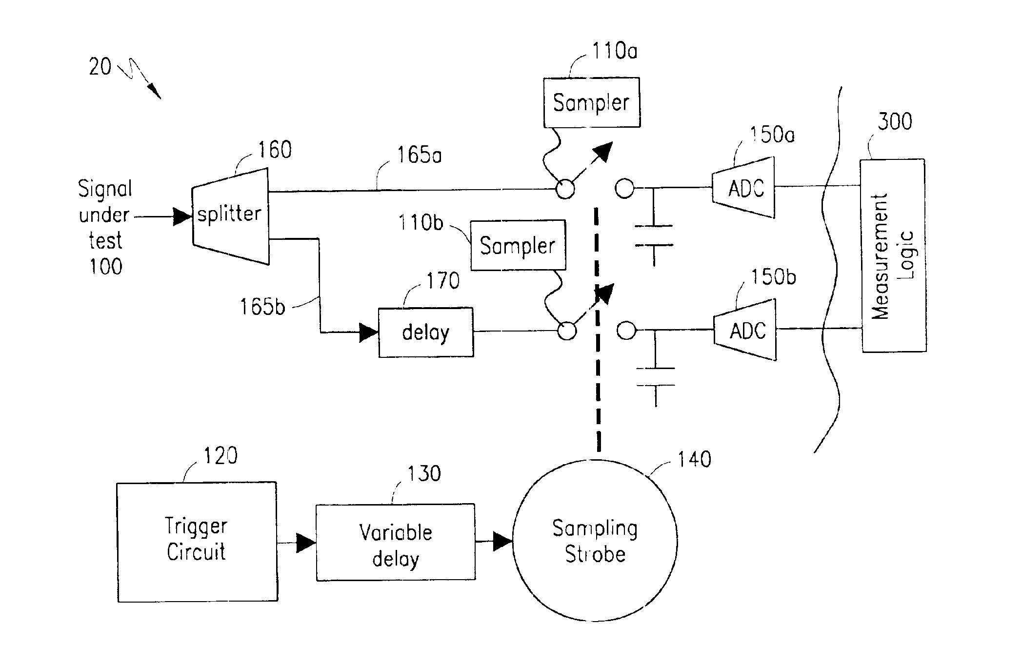
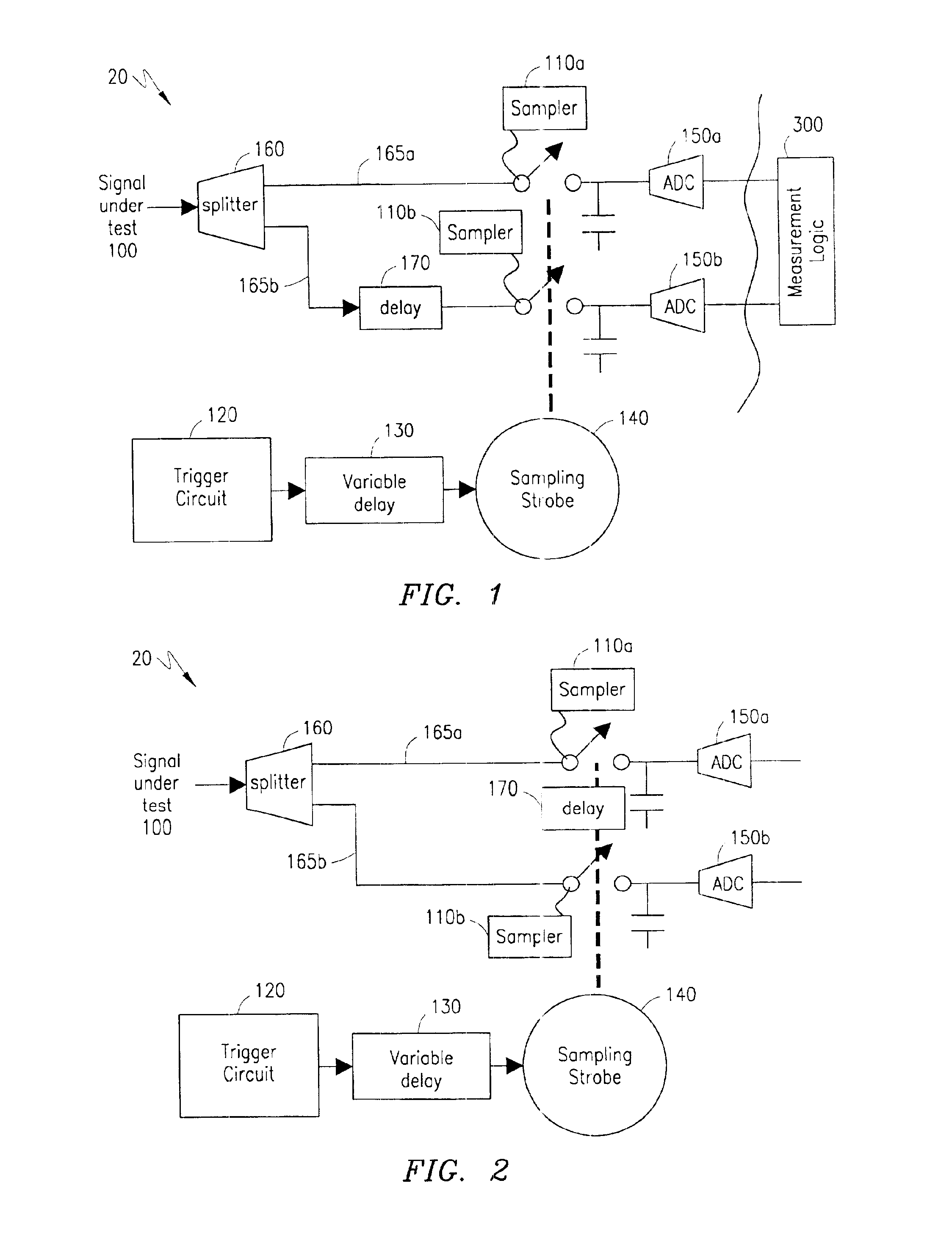
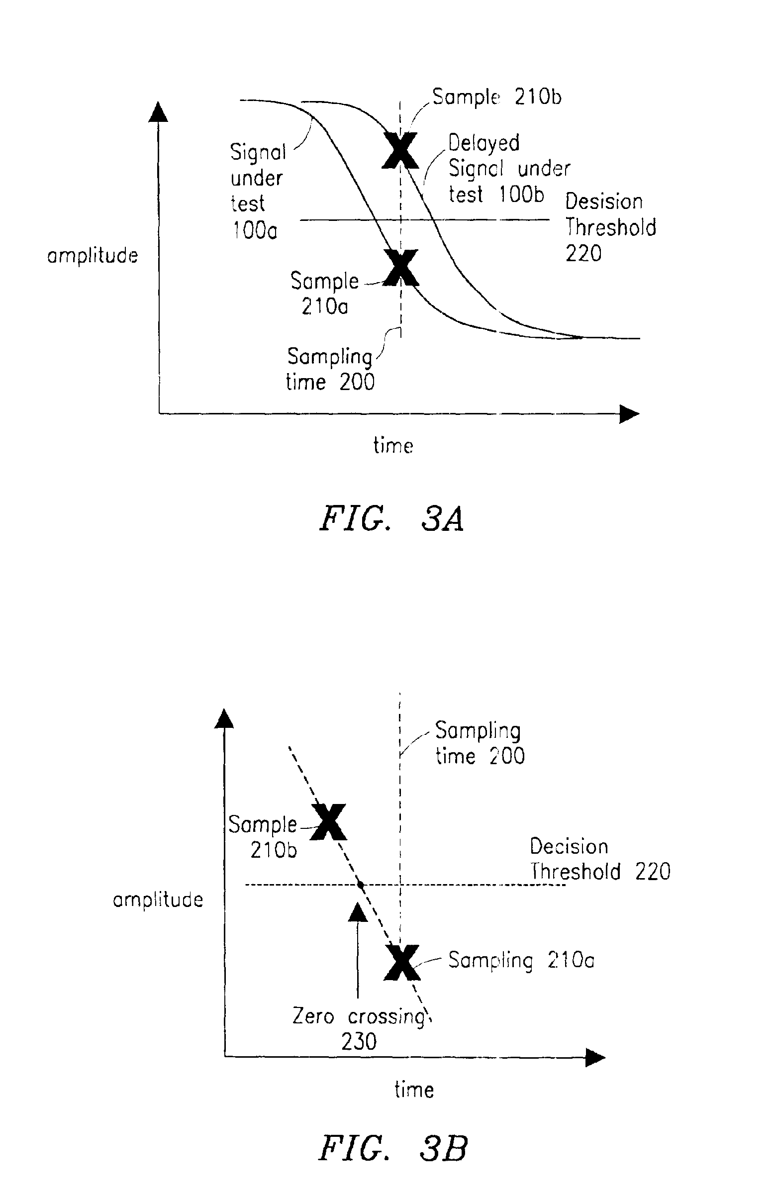
FIG. 1 illustrates an offset sampling apparatus 20 in accordance with embodiments of the present invention. The offset sampling apparatus 20 can be used, for example, in high-speed optical or electronic sampling oscilloscopes, to measure waveforms and zero-crossings of a signal-under-test (SUT) 100. A zero-crossing refers to the time that the amplitude of the SUT crosses a decision threshold (e.g., one-half amplitude) during a transition (e.g., from a “one” logic level to a “zero” or vice-versa) of the S...


PUM


Abstract

A sampling apparatus for use in high data rate jitter measurement systems based on offset sampling uses a trigger circuit, along with a time-based variable delay, to align a sampling strobe to drive two samplers. An input data signal is split and fed via separate signal paths into the two samplers. One of the samplers is delayed in sampling the input signal or the input is delayed to one of the samplers, such that the two samples of the input signal are offset in time. The jitter present in the SUT can be calculated using the two samples. In addition, when using two strobe circuits, the jitter inherently present in the strobe circuits can be compensated for by offset sampling a reference clock with each main strobe to determine the phase and cycle number of the reference clock at each strobe time.

Description

BACKGROUND OF THE INVENTION1. Technical Field of the InventionThe present invention relates generally to test and measurement systems, and specifically to measurement of the jitter in electrical and optical data streams.2. Description of Related ArtJitter is the deviation of the actual zero-crossing time of a signal from the ideal zero-crossing time. The signal zero-crossing time refers to the time that the amplitude of a data signal crosses a decision threshold (e.g., one-half amplitude) of a signal transition (e.g., a rise or fall of the signal). Measuring the jitter in serial data communications systems ensures that the jitter (if any) present in the system does not cause errors. There are a number of techniques for measuring jitter at lower frequencies. Examples of devices that have been used to measure the jitter in data streams include real-time digital oscilloscopes, phase-detector-based jitter measurement devices that include clock recovery circuits to convert the data strea...

Claims


Application Information

Patent Timeline
Patent Type & Authority Patents(United States)
IPC IPC(8): H04L1/20
CPCH04L1/205
Inventor CAMNITZ, LOVELL H.JUNGERMAN, ROGER L.KING, RANDALL
Owner AGILENT TECH INC
Why Eureka
Try Eureka