Non-contact tester for electronic circuits

a non-contact, tester technology, applied in the direction of electronic circuit testing, measurement devices, instruments, etc., can solve problems such as sometimes occurring damag

Inactive Publication Date: 2005-04-26
SCANIMETRICS
View PDF10 Cites 58 Cited by
  • Summary
  • Abstract
  • Description
  • Claims
  • Application Information

AI Technical Summary

Problems solved by technology

However, in making contact with the electronic circuit damages sometimes occurs when the mechanical probes make physical contact.

Method used


Image

  • Non-contact tester for electronic circuits
  • Non-contact tester for electronic circuits
  • Non-contact tester for electronic circuits

Examples


Embodiment Construction

[0011]The preferred embodiment, a non-contact tester for electronic circuits will now be described with reference to FIGS. 1 through 5.

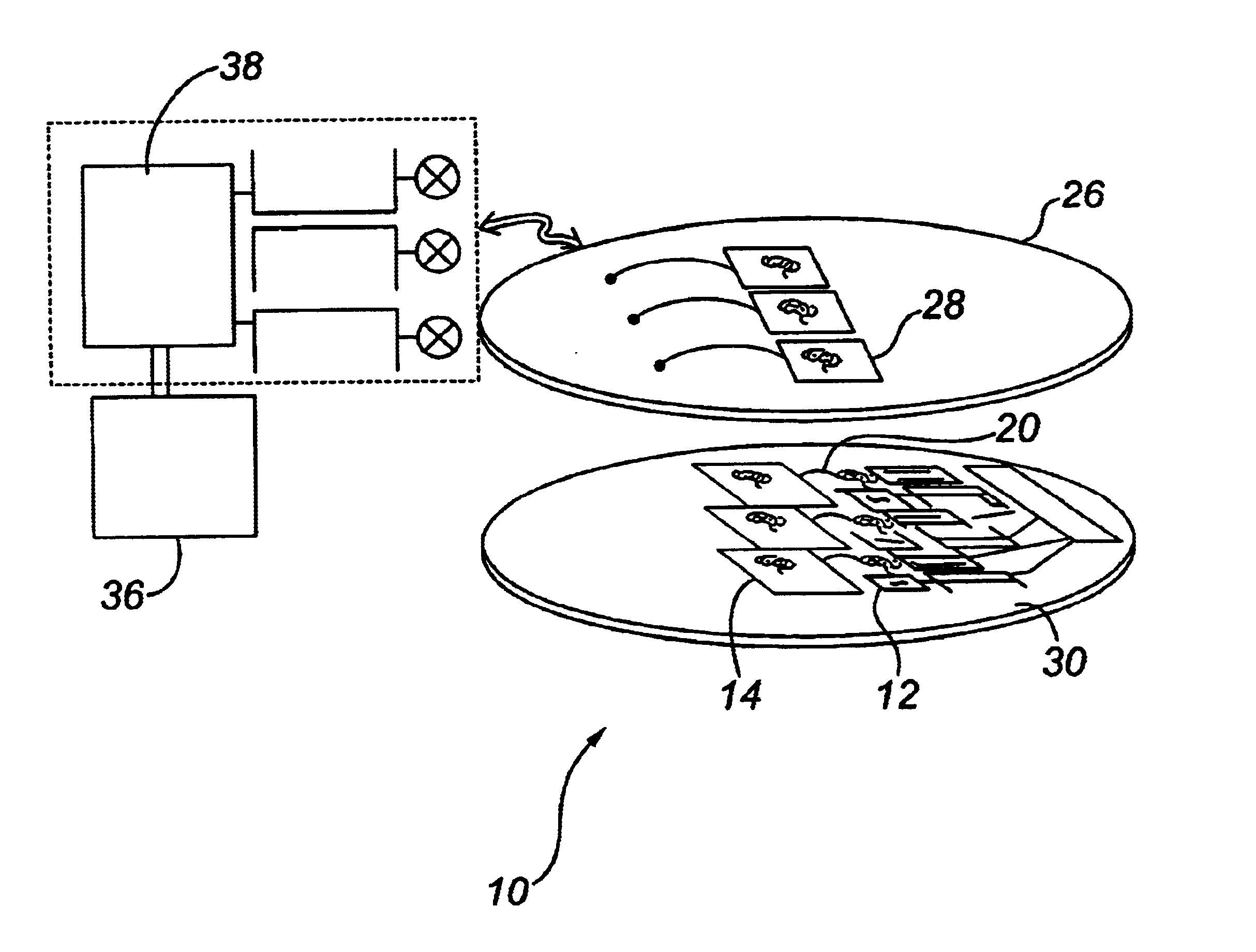
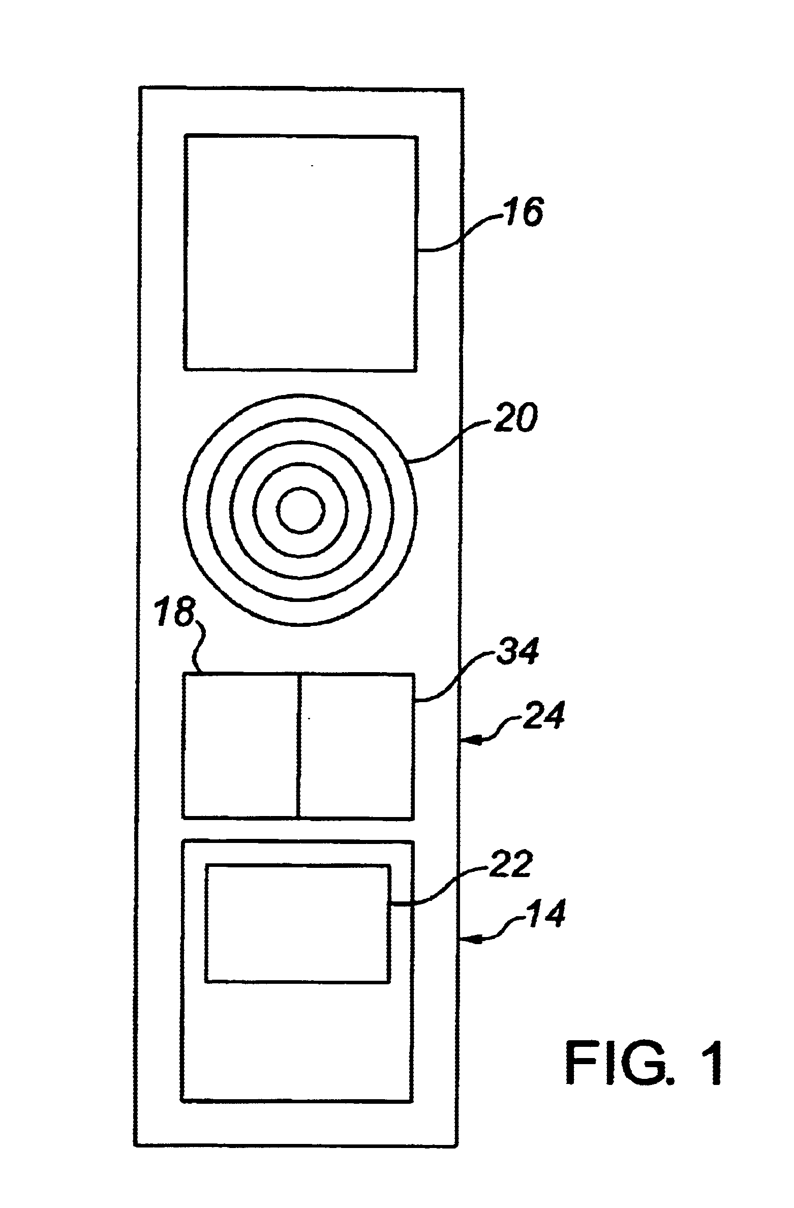
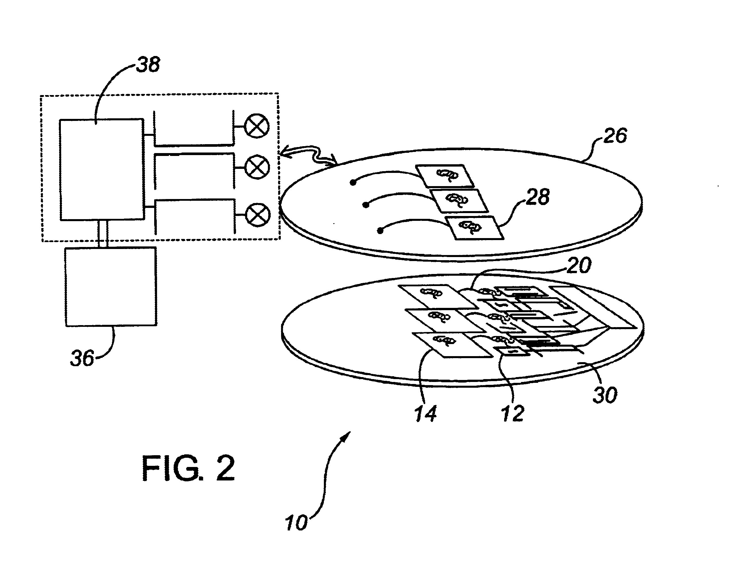
[0012]Referring to FIG. 2, there is provided a non-contact tester for electronic circuits, generally referenced by numeral 10. Non-contact tester 10 includes an electronic circuit 12 illustrated in FIG. 3 which has a wireless i / o cell 14. Referring to FIG. 1, in the illustrated embodiment, i / o cell 14 includes a bond pad 16, a transceiver 18, an antenna 20 and input / output elements 22, however, it will be appreciated that i / o cell 14 could work without a bond pad 16, or that antenna 20 could also function as a bond pad. Referring to FIG. 2, electronic circuit 12 also has a radio frequency interface generally referenced by numeral 24 for sending and receiving signals via wireless i / o cell 14 illustrated in FIG. 1.

[0013]Referring to FIG. 5, an independent scanning head generally referenced by numeral 26 is also provided. Independent scanning head 26 ha...


PUM


Abstract

A non-contact tester for electronic circuits consists of an electronic circuit and independent scanning head, in combination. The electronic circuit includes a micro-fabricated wireless i / o cell and means for sending and receiving signals via the wireless i / o cell. The independent scanning head has a wireless i / o cell that is compatible with the wireless i / o cell on the electronic circuit. This enables data to be exchanged with the electronic circuit to confirm proper functioning of the electronic circuit.

Description

FIELD OF THE INVENTION[0001]The present invention relates to testers for electronic circuits.BACKGROUND OF THE INVENTION[0002]Electronic circuits must be tested to ensure that they are not defective. At the present time this is done through the use of mechanical probes. The mechanical probes touch down on the electronic circuit and data is passed through the circuit. However, in making contact with the electronic circuit damages sometimes occurs when the mechanical probes make physical contact.SUMMARY OF THE INVENTION[0003]What is required is a tester for electronic circuits which is able to test the electronic circuits without making physical contact.[0004]According to the present invention there is provided a non-contact tester for electronic circuits which consists of an electronic circuit and independent scanning head, in combination. The electronic circuit includes a micro-fabricated wireless i / o cell and means for sending and receiving signals via the wireless contact. The ind...

Claims


Application Information

Patent Timeline
Patent Type & Authority Patents(United States)
IPC IPC(8): G01R31/303G01R31/28G01R31/315
CPCG01R31/303G01R31/3025G01R31/2822G01R31/315
Inventor SLUPSKY, STEVEN HAROLD
Owner SCANIMETRICS
Why Eureka
Try Eureka