Liquid crystal display device with substantially bilaterally symmetric pixel electrodes

a liquid crystal display and substantially bilateral technology, applied in non-linear optics, instruments, optics, etc., can solve the problems of inability to accurately detect the pixel electrodes and degrade the resolution of the lcd, and achieve the effect of improving the resolution characteristic, and sacrificing the storage capacitance or the aperture ratio

Inactive Publication Date: 2005-04-26
LG DISPLAY CO LTD
View PDF10 Cites 5 Cited by
  • Summary
  • Abstract
  • Description
  • Claims
  • Application Information

AI Technical Summary

Benefits of technology

[0014]An object of the present invention is to provide a liquid crystal display (LCD) having an improved resolution characteristic.
[0015]Another object of the present invention is to provide a liquid crystal display (LCD) having an improved resolution characteristic without sacrificing the storage capacitance or the aperture ratio.

Problems solved by technology

However, due to its large weight and size, the CRT has been inapt for effectively responding to recent demands for downsizing and weight reduction of electronic appliances.
The LCD of the related art suffers a drawback that,,when the LCD is operated in a dot inversion mode, the resolution of the LCD degrades.

Method used


Image

  • Liquid crystal display device with substantially bilaterally symmetric pixel electrodes
  • Liquid crystal display device with substantially bilaterally symmetric pixel electrodes
  • Liquid crystal display device with substantially bilaterally symmetric pixel electrodes

Examples


first embodiment

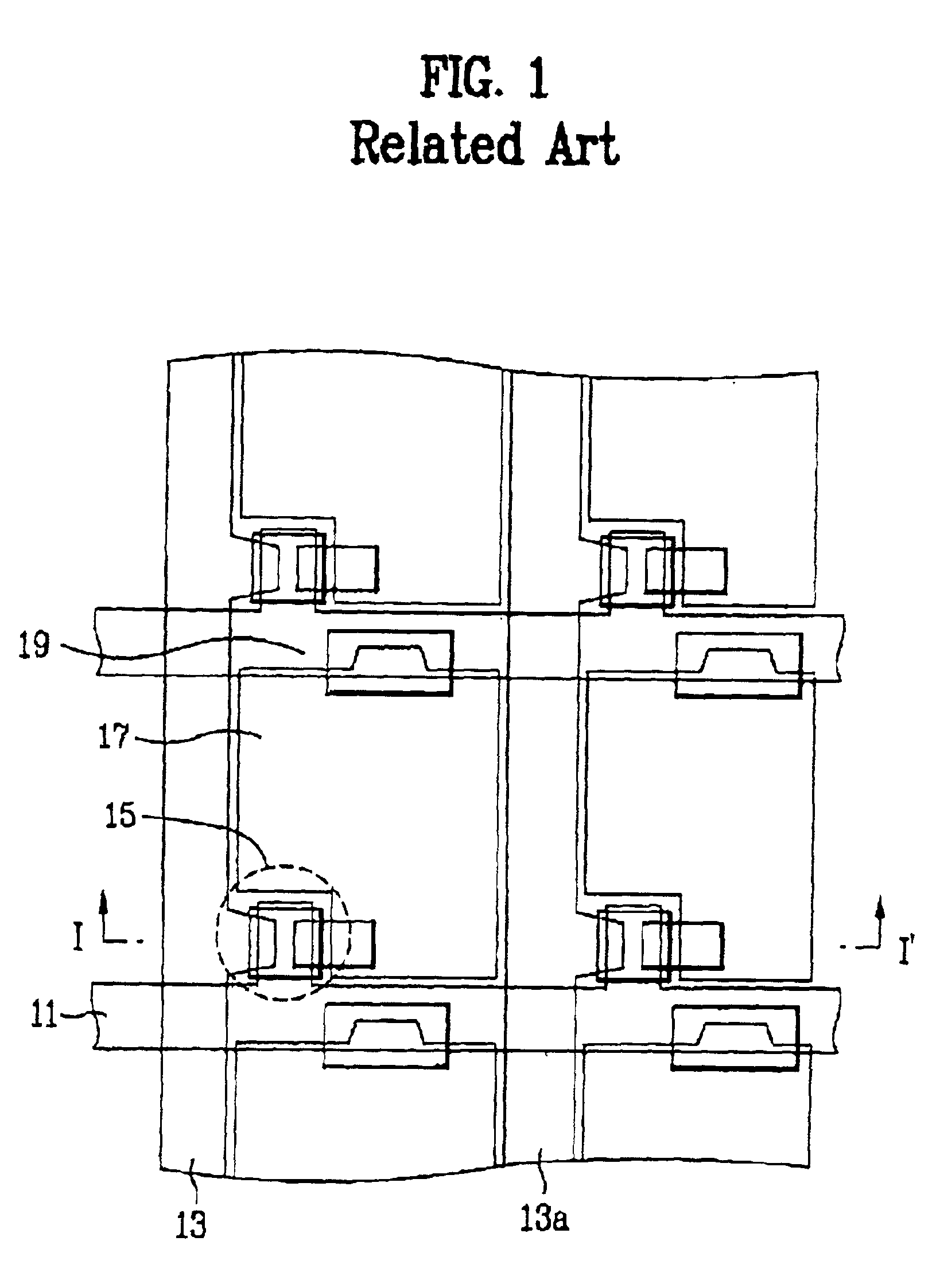
[0037]FIG. 4 is a layout view of an LCD according to a first embodiment of the present invention. FIG. 5 is a sectional view taken along the line II-II′ of FIG. 4. As shown in FIG. 4, the LCD of this example includes a plurality of scan lines 41n-1 and 41n extending in one direction and a plurality of data lines 43n-1 and 43n extending in a direction intersecting the scan lines. The scan lines and the data lines define pixel areas. Thin film transistors (TFTs) 45 each have a gate electrode, and a source electrode and a drain electrode are formed adjacent the intersecting portions of the scan lines and the data lines. In each of the TFTs 45, the gate electrode is branched off from an adjacent one of the scan lines, and the source electrode extends from an adjacent one of the data lines. The pixel areas are provided with pixel electrodes 47 connected with the respective drain electrodes via contact holes (not shown in the figures). Each of electrodes 49 serves as an electrode of the c...

second embodiment

[0042]A second embodiment of the present invention has a structure that enables efficient utilization of the removed portions at the lower right parts of ITOs (pixel electrodes) in the first embodiment. Specifically, electrodes of storage capacitors are extended to the removed lower right part of the ITOs (pixel electrodes) of the previous row to increase the storage capacitance. This in turn enables a reduction of the width of the scan lines, which helps improve the aperture ratio of the LCD panel, as explained below in more detail.

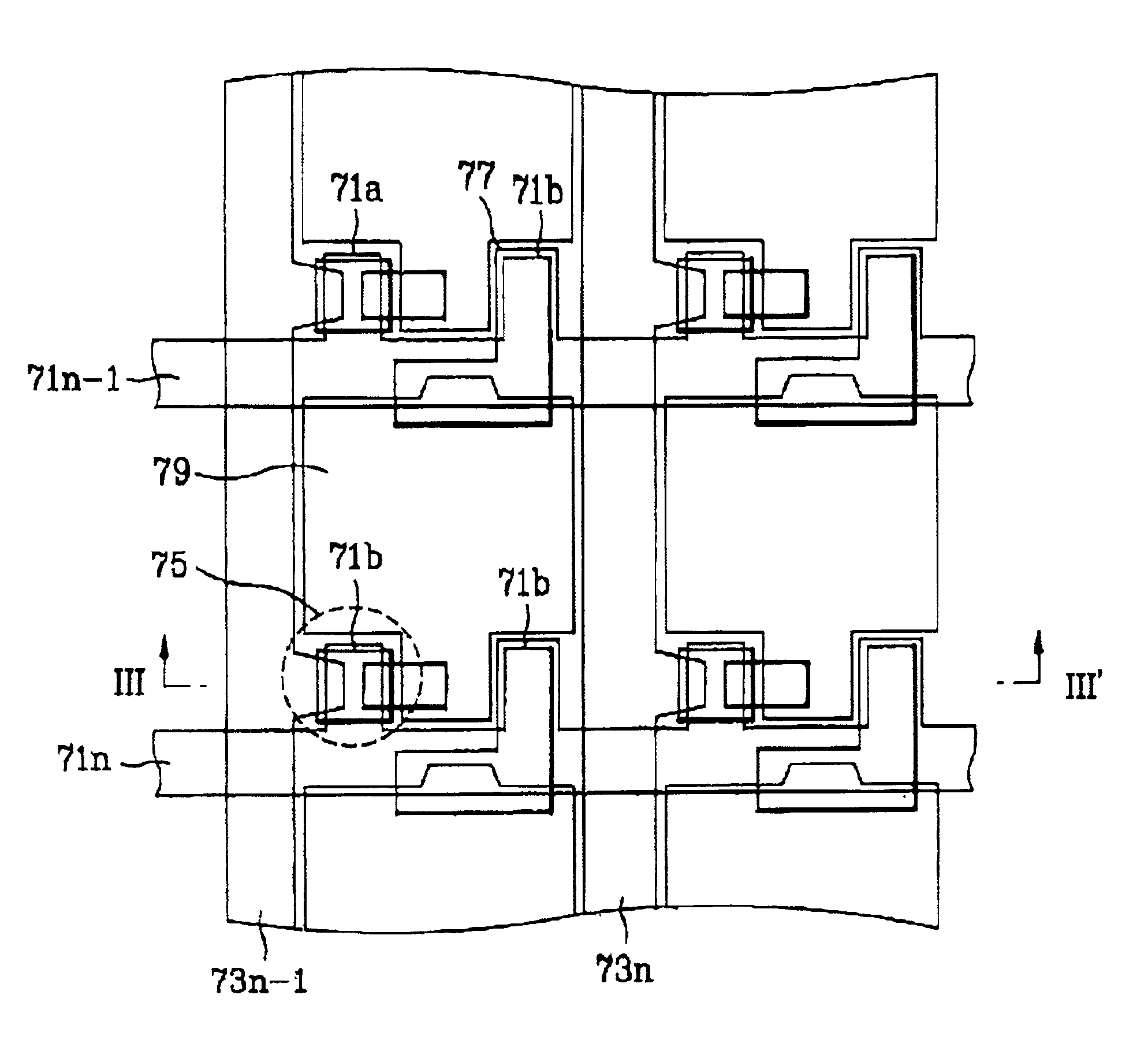
[0043]FIG. 7 is a layout view of an LCD according to the second embodiment of the present invention, and FIG. 8 is a sectional view taken along the line III-III′ of FIG. 7.

[0044]As shown in FIG. 7, the LCD according to the second embodiment of the present invention includes scan lines 71n-1 and 71n extending in one direction. Each of the scan lines has first and second projections 71a and 71b with a spacing therebetween in each pixel area. The LCD of thi...


PUM

PropertyMeasurementUnit
widthaaaaaaaaaa
areaaaaaaaaaaa
areasaaaaaaaaaa

Abstract

A liquid crystal device (LCD) includes a first substrate; a second substrate coupled to the first substrate; a plurality of scan lines and a plurality of data lines arranged over the first substrate, the scan lines intersecting the data lines to define pixel areas; thin film transistors (TFTs) over the first substrate adjacent intersections of the scan lines and data lines; substantially bilaterally symmetric pixel electrodes in the pixel areas; and a liquid crystal layer interposed between the first and second substrates.

Description

[0001]This application claims the benefit of Korean Application No. P 2000-38015, filed in Korea on Jul. 4, 2000, which is hereby incorporated by reference.BACKGROUND OF THE INVENTION[0002]1. Field of the Invention[0003]The present invention relates to a display device, and more particularly, to a liquid crystal display device.[0004]2. Discussion of the Related Art[0005]Among various display devices, a cathode tube ray (CRT) has been widely used for monitors in television, measuring instrument and digital assistant equipment. However, due to its large weight and size, the CRT has been inapt for effectively responding to recent demands for downsizing and weight reduction of electronic appliances.[0006]A liquid crystal display (LCD), which is advantageously light weighted and small sized, has been actively developed in an effort to replace the CRT. According to the recent development, the LCD can sufficiently function as a flat display device, and the demand therefor is increasing.[00...

Claims


Application Information

Patent Timeline
Patent Type & Authority Patents(United States)
IPC IPC(8): G02F1/13G02F1/1343G02F1/1362G02F1/136
CPCG02F1/134336G02F1/136213G02F2201/123G02F1/136
Inventor CHUNG, IN JAEPARK, JUNE HO
Owner LG DISPLAY CO LTD
Why Eureka
Try Eureka