Trench capacitor with pillar

a trench capacitor and capacitor plate technology, applied in the direction of semiconductor devices, electrical apparatus, transistors, etc., can solve the problems of increasing the difficulty of trench capacitors having the capacitance required for circuit requirements, increasing the difficulty of manufacturing trench capacitors, and increasing the difficulty of processing, so as to increase the surface area of capacitor plates, increase the capacitance, and increase the effect of surface area

Inactive Publication Date: 2005-03-03
INFINEON TECH AG +1
View PDF0 Cites 18 Cited by
  • Summary
  • Abstract
  • Description
  • Claims
  • Application Information

AI Technical Summary

Benefits of technology

These and other problems are generally solved or circumvented, and technical advantages are generally achieved, by preferred embodiments of the present invention, which provide a capacitor having an increased surface area of the plates. A pillar is formed in the center of the trench that is electrically connected to the buried plate or outer capacitor plate in the bottom of the trench. Thus, the surface area of the capacitor plates is increased, providing increased capacitance without increasing the depth or width of the trench.
Advantages of preferred embodiments of the present invention include increasing the surface area of capacitor plates, thus increasing the capacitance. The capacitance of a trench capacitor can be doubled, resulting in the ability to manufacture shallower, narrower trenches without sacrificing capacitance. Manufacturing a trench capacitor having a pillar inside the trench as described herein results in the ability to reduce the ground rules or place more trenches into the same unit area. In one embodiment, the conductive pillar is hollow, further increasing the surface area of the capacitor plates and thus further increasing, e.g., almost tripling, the capacitance. Embodiments of the present invention are particularly advantageous in scaled-down memory devices having ground rules of less than about 0.15 μm, for example.

Problems solved by technology

However, as ground rules are scaled or reduced, it becomes more and more difficult to manufacture trench capacitors having the capacitance required for the circuit requirements.
For example, the trenches generally have high aspect ratios, which are more difficult to process, and the lateral surface area of the chip surface area needs to be conserved.

Method used


Image

  • Trench capacitor with pillar
  • Trench capacitor with pillar
  • Trench capacitor with pillar

Examples


Embodiment Construction

The making and using of the presently preferred embodiments are discussed in detail below. It should be appreciated, however, that the present invention provides many applicable inventive concepts that can be embodied in a wide variety of specific contexts. The specific embodiments discussed are merely illustrative of specific ways to make and use the invention, and do not limit the scope of the invention.

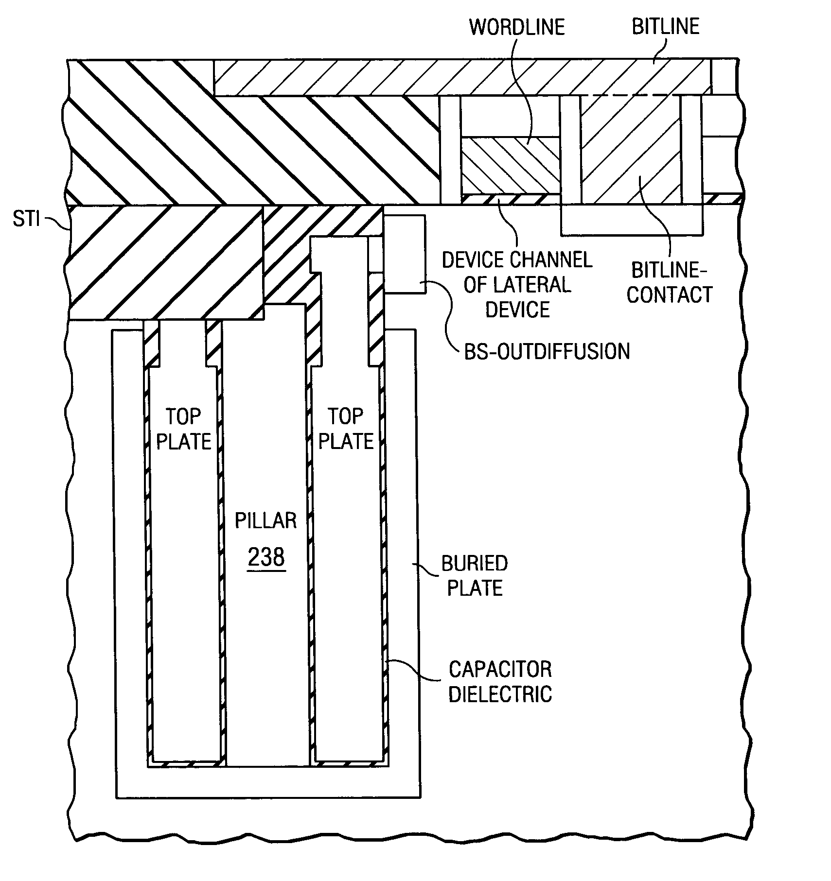
The present invention will be described with respect to preferred embodiments in a specific context, namely a DRAM device. The invention may also be applied, however, to other memory devices and semiconductor applications requiring or utilizing trench capacitors. A cross-sectional view of one capacitor is shown in each figure, although many other capacitors and components may be present in the semiconductor devices shown.

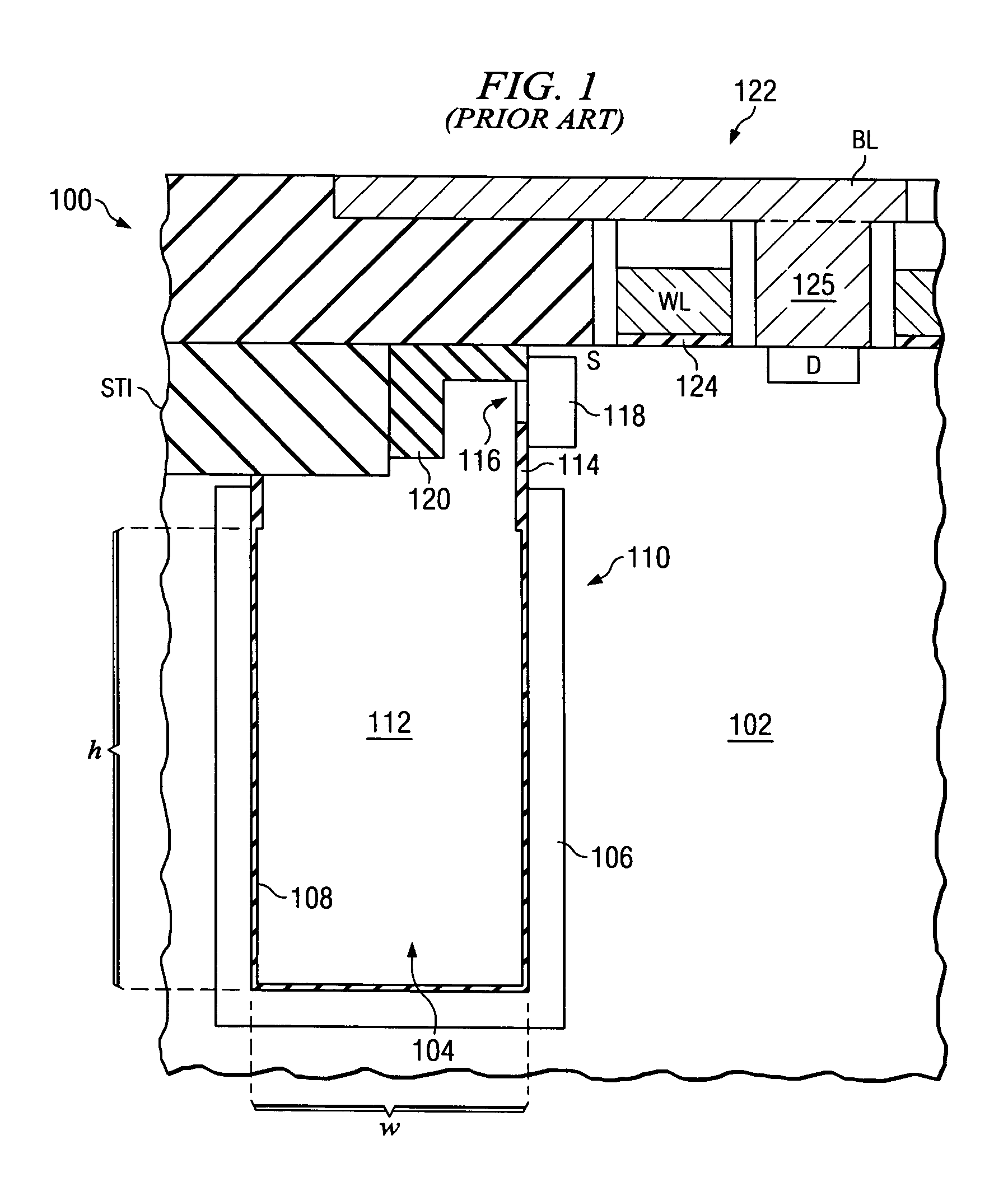
With reference now to FIG. 1, a prior art trench DRAM device 100 having a lateral access device 122 is shown. A trench 104 is formed in a substrate 102. A top...


PUM


Abstract

A trench capacitor having a conductive pillar in a central region of a trench. A first plate of the capacitor includes the substrate in the lower portion of the trench and the conductive pillar. The capacitor dielectric is disposed over the conductive pillar and the sidewalls of the trench lower portion. A second plate of the capacitor is a conductive material disposed over the dielectric material. The conductive pillar increases the surface area of the capacitor plates, increasing the capacitance of the capacitor. A top portion of the conductive pillar may be hollow, further increasing the surface area of the capacitor plates.

Description

TECHNICAL FIELD The present invention relates generally to the fabrication of semiconductor devices, and more particularly to the fabrication of capacitors. BACKGROUND Semiconductor devices are used in a variety of electronic applications, such as personal computers and cellular phones, for example. One such semiconductor product widely used in electronic systems for storing data is a semiconductor memory device, and a common type of semiconductor memory is a dynamic random access memory (DRAM). A DRAM typically includes millions or billions of individual DRAM cells arranged in an array, with each cell adapted to store one bit of data. A DRAM memory cell typically includes an access field effect transistor (FET) and a storage capacitor. The access FET allows the transfer of data charges to and from the storage capacitor during reading and writing operations. In addition, the data charges on the storage capacitor are periodically refreshed during a refresh operation. DRAM storage...

Claims


Application Information

Patent Timeline
Patent Type & Authority Applications(United States)
IPC IPC(8): H01L21/334H01L21/8234H01L21/8242H01L21/8244H01L27/108H01L29/94
CPCH01L27/10864H01L29/945H01L29/66181H01L27/1087H10B12/0383H10B12/0387
Inventor RUPP, THOMAS STEFFENKUDELKA, STEPHANMICHAELIS, ALEXANDERRADENS, CARL J.
Owner INFINEON TECH AG
Why Eureka
Try Eureka