
All digital PLL trimming circuit

a technology of all digital and phaselocked loops, applied in the direction of electrical equipment, pulse automatic control, etc., can solve the problems of affecting the filtration of reference frequency, unwanted side effects, and the introduction of pll phase noise due to the vco, and achieve the effects of wide gain change, increased locking speed, and frequency differen

Inactive Publication Date: 2005-05-31
MICROCHIP TECH INC
View PDF15 Cites 23 Cited by
  • Summary
  • Abstract
  • Description
  • Claims
  • Application Information

AI Technical Summary

Benefits of technology

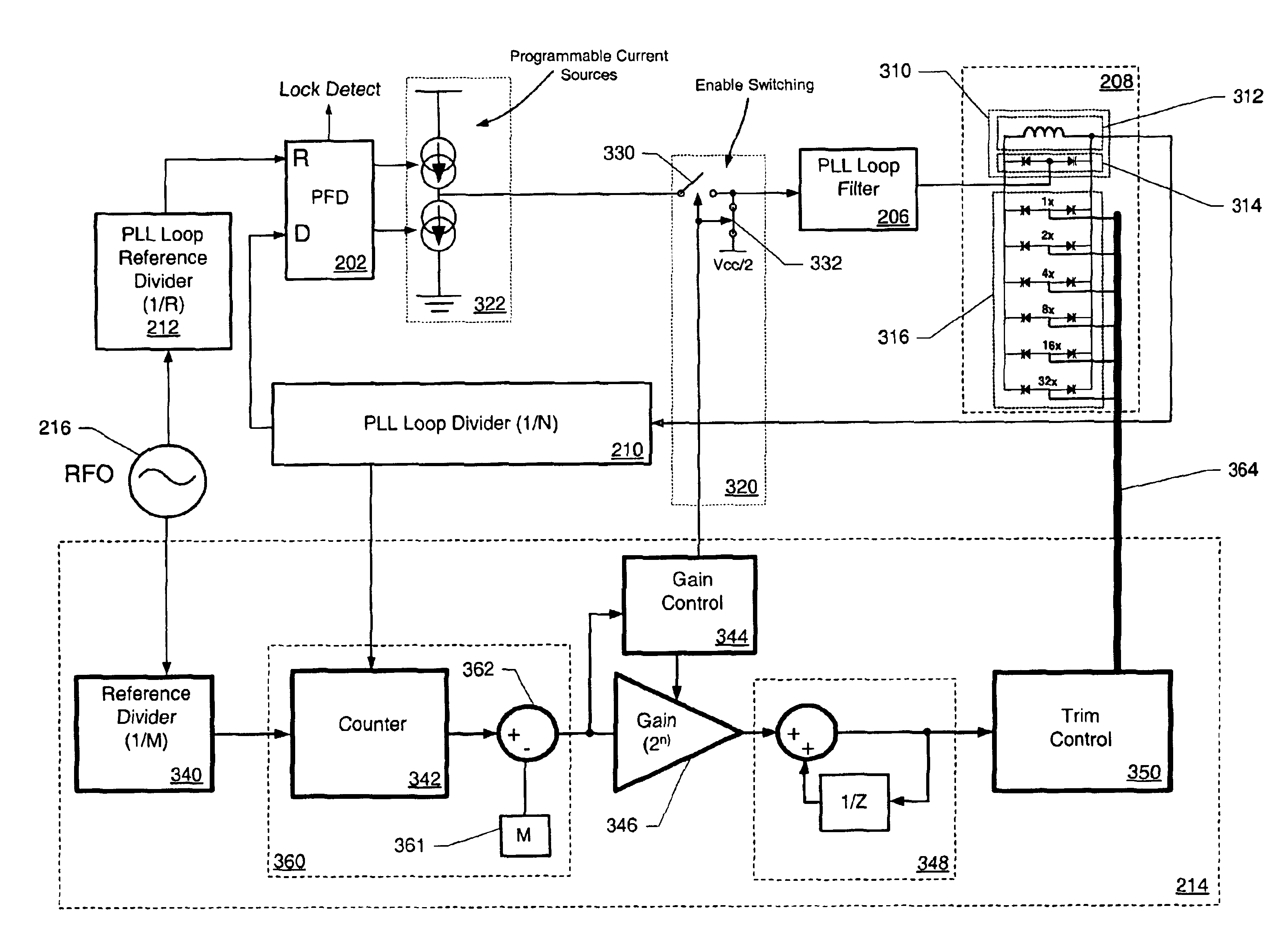
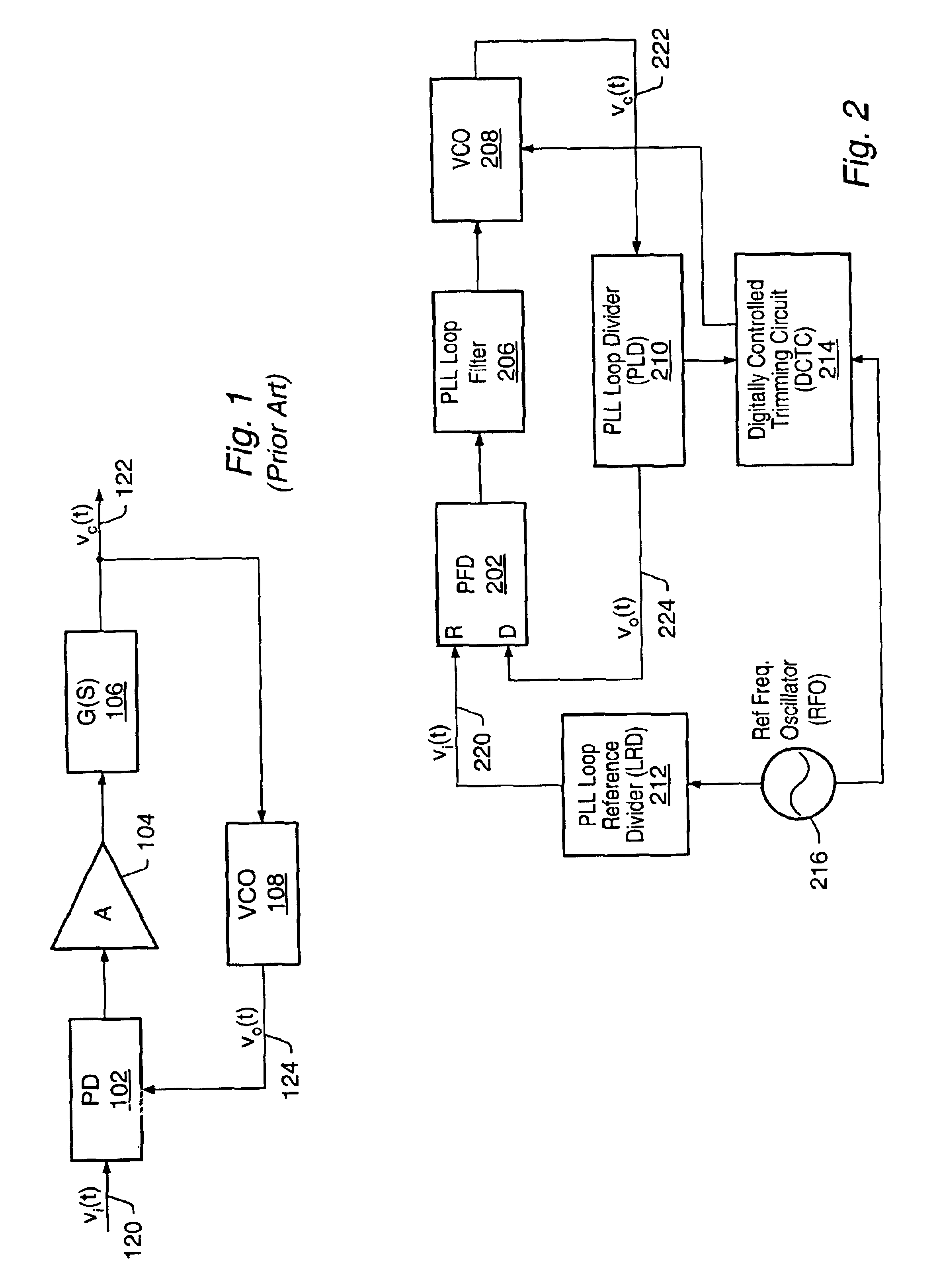
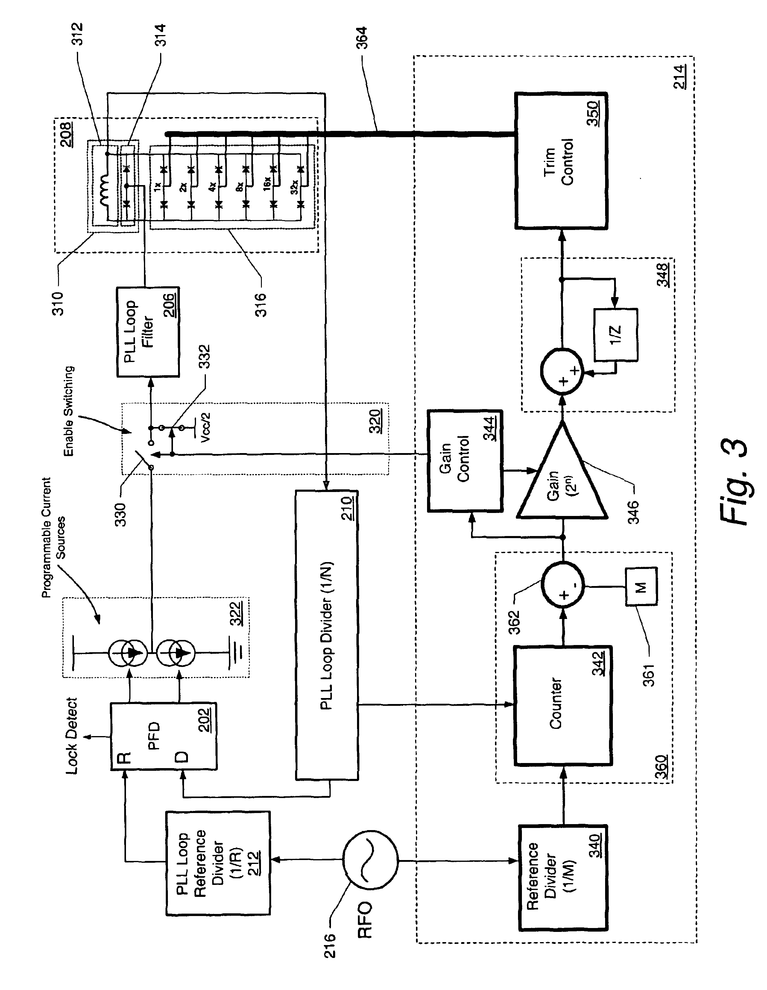
[0010]In one set of embodiments the invention comprises a system and method for automatically trimming the center frequency of a VCO in a PLL. The trimming may be performed by a digitally controlled trimming circuit (DCTC), which may be used as part of a clock recovery architecture or as part of a high-end PLL. It may also be used by itself in low-end PLLs, and may be operated to change the gain of the VCO. In one embodiment, a second loop based solely on the frequency difference between a reference frequency and a divided output frequency of the VCO is introduced into the main PLL loop. This frequency loop, also referred to as a trimming loop, may be optimized by the inclusion of a gain control stage, which may lower the locking time. A control module may be introduced to delay the deployment of the phase detector until the frequency loop has fully converged, that is until trimming has been completed, thus preventing the two loops from interfering with each other.
[0014]The frequency difference between the trimming loop and the main PLL loop may be made very small. This may help eliminate the phase slips, and thus many non-linear acquisition characteristics typically present in traditional PLLs. Embodiments of the present invention may also provide increased locking speed when contrasted with a typical PLL. In one embodiment, the trimming loop may be optimized to have a locking time spanning less than eight cycles, over a very wide gain change. Also, the counter cycle may be made faster than the reference frequency at the phase detector. Due to the small change in frequency between the loop frequency at the time of release of the trimming loop and the final PLL frequency, the overall lock time may be substantially reduced. (The loop settling time for a given phase margin may be given as a function of the frequency step). This may prove useful in clock recovery loops where filtration of the reference frequency may require small bandwidth loops at the expense of locking time.
[0015]Thus, various embodiments of the invention may provide a means for automatically trimming the center frequency of a VCO in a PLL using a digitally controlled trimming circuit configured in a second loop based solely on the frequency difference between a reference frequency and a divided output frequency of the VCO, thus reducing phase noise and increasing the range of the main PLL loop, while also providing a faster locking time.

Problems solved by technology

One problem associated with PLLs and PLL design is the introduction of PLL phase noise due to the VCO.
Generally, the non linear nature of the phase frequency detector in the PLL and the limited bandwidth of the PLL itself may result in unwanted side effects when utilizing control voltage based solutions.
Thus, while opening the loop bandwidth may present a solution, the reference frequency filtration will suffer.
At the same time, the presence of phase slips in the lock acquisition phase can further slow down the decision point.
If there is an excessive difference between the two input terminals of the phase detector, a phase slip may occur in which the detector generally pumps in the wrong direction.
However, by definition, the reference and feedback inputs of the phase detector must accumulate enough phase error to trigger this event.
Therefore, as the frequency error between the two input terminals is reduced, the rate of the phase slips is reduced as well, thus providing an inconsistent locking time.

Method used


Image

  • All digital PLL trimming circuit
  • All digital PLL trimming circuit
  • All digital PLL trimming circuit

Examples


Embodiment Construction

[0025]As used herein, a “trigger” signal is defined as a signal that is used to initiate, or “trigger”, an event or a sequence of events in a digital system. A trigger signal is said to be in a “triggering state” at a time when it initiates a desired event, or sequence of events. A periodic trigger signal may commonly be referred to as a “clock”. In a “synchronous” digital system, generally a clock, commonly referred to as a “system clock”, may be used for initiating most events, or sequences of events. An example of a triggering state may be, but is not limited to, a rising edge of a pulse of a clock in a synchronous digital system.

[0026]When an event, or a sequence of events, is said to be initiated “in response to” receiving a stimulus signal, it may be implied that the event, or the sequence of events, is initiated as a result of a combination of a trigger signal, used in triggering the event or sequence of events, being in a triggering state at a time when the stimulus signal i...


PUM


Abstract

In one set of embodiments, the invention comprises a system and method for automatically trimming the center frequency of a VCO in a PLL. The trimming may be performed by a digitally controlled trimming circuit, which may be operated to modify a gain of the VCO and may be used as part of a clock recovery architecture or as part of a high-end PLL. It may also be used by itself in low-end PLLs. In one embodiment, a second loop based solely on the frequency difference between a reference frequency and a divided output frequency of the VCO is introduced into the PLL loop. This frequency loop may be optimized by the inclusion of a gain control stage, which may lower the locking time. A control module may also be introduced to delay the deployment of the phase detector until the frequency loop has fully converged, that is until trimming has been completed, thus preventing the two loops from interfering with each other and compromising each other's performance.

Description

BACKGROUND OF THE INVENTION[0001]1. Field of the Invention[0002]This invention relates generally to the field of analog and / or digital circuit design and, more particularly, to phase-locked loop (PLL) design.[0003]2. Description of the Related Art[0004]A phase-locked loop (PLL) is an electronic circuit, in which a voltage- or current-driven oscillator is constantly being adjusted to lock on (or match in phase) the frequency of an input signal. Therefore, PLLs are useful for providing stability for communications channels by keeping them set to specific respective frequencies. In addition, PLLs are also used for generating signals, modulating or demodulating signals, reconstituting a particular signal with less noise, or multiplying / dividing a frequency. In general, PLLs are widely used in applications requiring a high degree of noise immunity and narrow bandwidth, for example wireless communications that employ signal-carrying methods of phase modulation (PM), frequency modulation (...

Claims


Application Information

Patent Timeline
Patent Type & Authority Patents(United States)
IPC IPC(8): H03L7/06H03L7/087H03L7/113H03L7/191
CPCH03L7/087H03L7/191H03L7/113
Inventor BRIONES, LUIS J.
Owner MICROCHIP TECH INC
Learn More