Periodical precomputation and skew compensation circuit and method for delaying locking loop in FPGA chip thereof

A pre-calculation and periodic technology, applied in the direction of electrical components, automatic power control, etc., can solve the problems of large resource consumption and long lock time, and achieve the effect of balancing phase lock time, shortening lock time, and improving clock management performance

CN103905038AInactive Publication Date: 2014-07-02SOUTHEAST UNIV
6 Cites 15 Cited by

Patent Information

Authority / Receiving Office
CN · China
Current Assignee / Owner
Publication Date
2014-07-02
Estimated Expiration
Not applicable · inactive patent

Smart Images

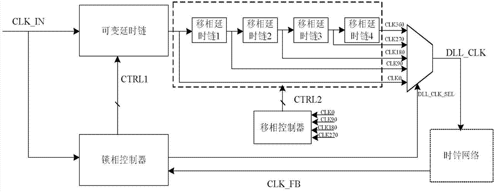
  • Figure 1
    Figure 1
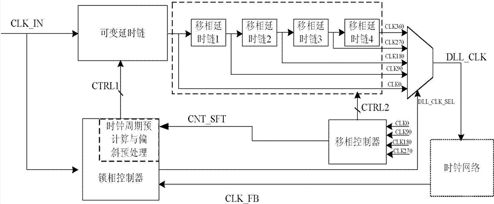
  • Figure 2
    Figure 2
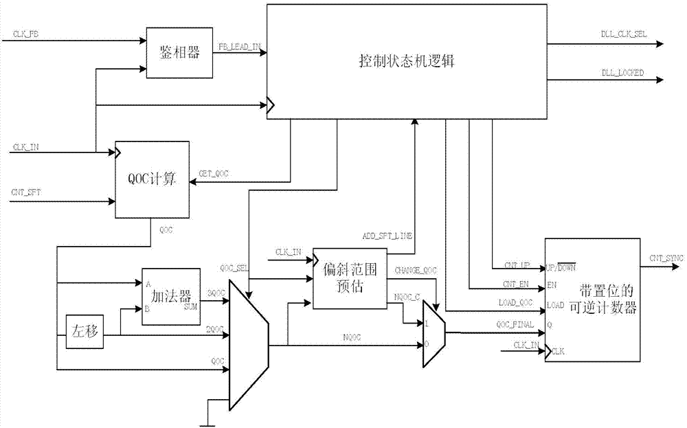
  • Figure 3
    Figure 3
Patent Text Reader

Abstract

The invention discloses a periodical precomputation and skew compensation circuit and a method for delaying a locking loop in a FPGA chip of the periodical precomputation and skew compensation circuit. On the basis of an original traditional DLL locking method, the periodical precomputation technology and the skew preprocessing technology are adopted for two-level processing of clock skew in the FPGA chip, and under the conditions that system stability is maintained and hardware expenses are not increased, the clock skew is removed rapidly, and locking is achieved. According to the method, in the phase locking process of a DLL structure, first-level digital logic computes and loads a preprocessed skew value according to periodical information digitized by a phase shift delay link, and then clock locking is completed by means of second-level counting approximation processing based on the preprocessed skew value. By means of the method, locking time can be effectively shortened, the method is particularly suitable for an occasion with a high demand for low-frequency skew compensation, phase locking time within a DLL operating frequency range can be balanced, and FPGA internal clock management performance can be improved.
Need to check novelty before this filing date? Find Prior Art

Description

technical field

[0001] The invention relates to the technical field of integrated circuit design, and is used to improve the internal digital clock management method of a Field Programmable Logic Array (FPGA) chip, in particular to an FPGA on-chip delay-locked loop method based on cycle pre-calculation skew compensation and cycle pre-calculation The skew compensation circuit is mainly to propose a new improvement method for the long locking time consumed by the internal DLL of the FPGA chip to remove the clock skew in the clock system, and the existing DLL improvement structure scheme consumes a lot of resources. Background technique

[0002] Acronyms and key term definitions

[0003]

[0004] Clock skew: In a synchronous digital system, the difference in time between clock edges arriving in different spaces;

[0005] Clock Skew Compensation: The delay-locked loop circuit is used to introduce some additional delay, so that the introduced delay plus the original clock ske...

Examples

Embodiment Construction

[0067] Below in conjunction with specific embodiment, further illustrate the present invention, should be understood that these embodiments are only used to illustrate the present invention and are not intended to limit the scope of the present invention, after having read the present invention, those skilled in the art will understand various equivalent forms of the present invention All modifications fall within the scope defined by the appended claims of the present application.

[0068] Such as Figure 2-3 As shown, the DLL is based on the phase-locked controller of the period pre-calculation and skew compensation control circuit inside the DLL. The circuit structure includes: QOC calculation circuit module, left shifter, adder, four-to-one multiplexer, two-to-one multiplexer , Skew range estimation circuit, reversible counter with setting, phase detector and control state machine logic;

[0069]The QOC calculation circuit module inputs the phase-shift delay link input ad...