Pll circuit
a phase lock loop and circuit technology, applied in the direction of electrical equipment, pulse automatic control, etc., can solve the problems of jitter, negative influence of lock lock stability, and inability to properly switch the charge pump current, so as to reduce the reference leakage, reduce the lock-up time, and the effect of well-balanced manner
- Summary
- Abstract
- Description
- Claims
- Application Information
AI Technical Summary
Benefits of technology
Problems solved by technology
Method used
Image
Examples
embodiment 1
[PLL Circuit]
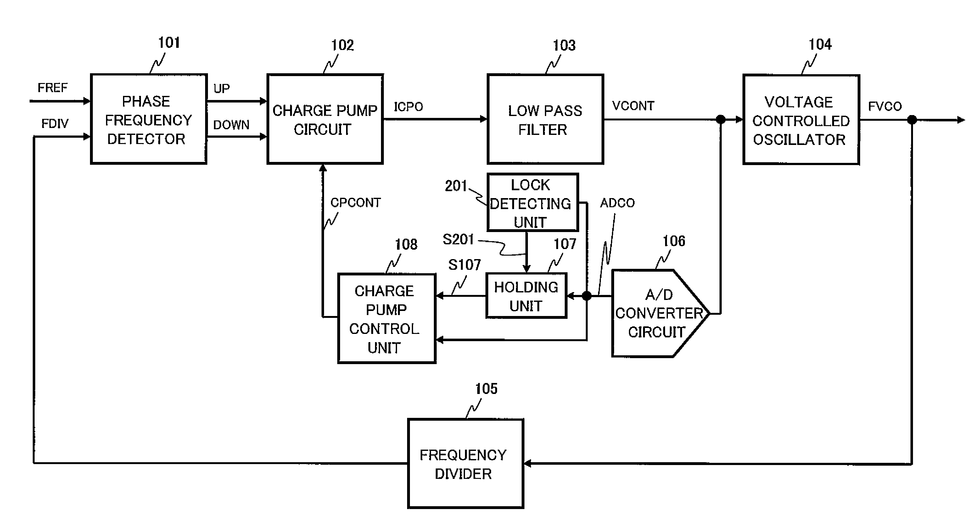
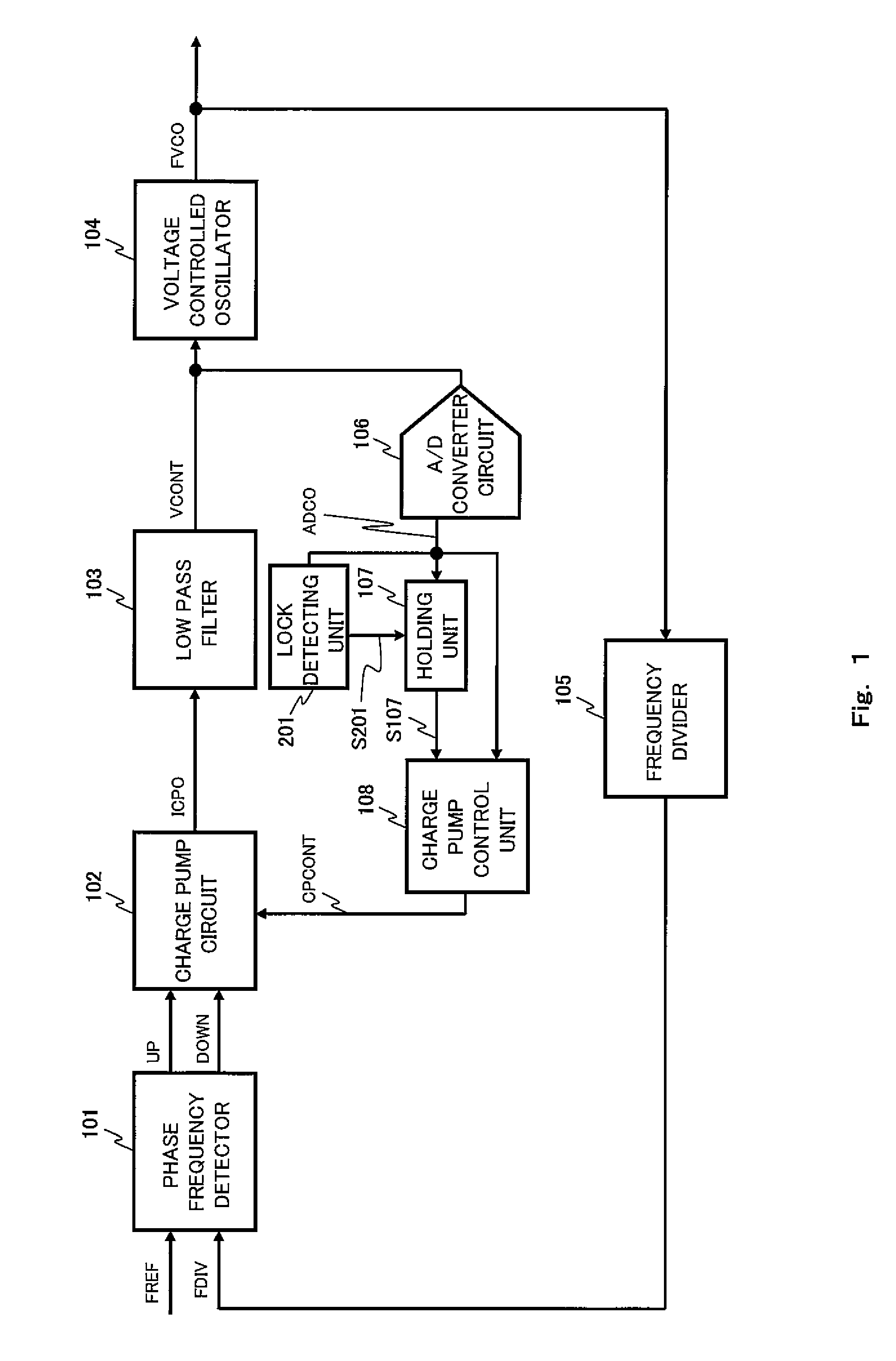
[0039]Hereinafter, a configuration of a PLL circuit according to Embodiment 1 of the present invention will be described with reference to FIG. 1.
[0040]FIG. 1 is a block diagram showing the configuration of the PLL circuit according to Embodiment 1 of the present invention. Referring to FIG. 1, the PLL circuit includes a phase frequency detector 101, a charge pump circuit 102, a low pass filter 103, a voltage controlled oscillator 104, a frequency divider 105, an analog / digital (A / D) converter circuit 106, a lock detecting unit 201, a holding unit 107, and a charge pump control unit 108.
[0041]The phase frequency detector 101 detects a phase difference and a frequency difference between a reference clock signal FREF and a feedback clock signal FDIV, and outputs an up-pulse signal UP and a down-pulse signal DOWN which are used for controlling the charge pump circuit 102 in accordance with the phase difference and the frequency difference. To be specific, when a phase of t...
embodiment 2
[0059]Hereinafter, a PLL circuit according to Embodiment 2 of the present invention will be described with reference to FIG. 6.
[0060]The configuration of the PLL circuit of Embodiment 2 is identical to that of the PLL circuit of Embodiment 1 of FIG. 1 except that the charge pump current amount is switched from an initial current amount to a current amount less than the initial current amount in multi-levels which are three levels or more, after a time point when the digital signal ADCO first becomes equal to the lower limit threshold or the upper limit threshold.
[0061]To be specific, as shown in FIG. 6, the charge pump control unit 108 switches the current amount from the first current amount Icp1 to the second current amount Icp2 less than the first current amount Icp1 when the digital signal ADCO becomes equal to the lower limit threshold (when it reaches (falls into) the lock detection range). Following this, the charge pump control unit 108 switches the current amount from the s...
embodiment 3
[0063]Hereinafter, a PLL circuit according to Embodiment 3 of the present invention will be described.
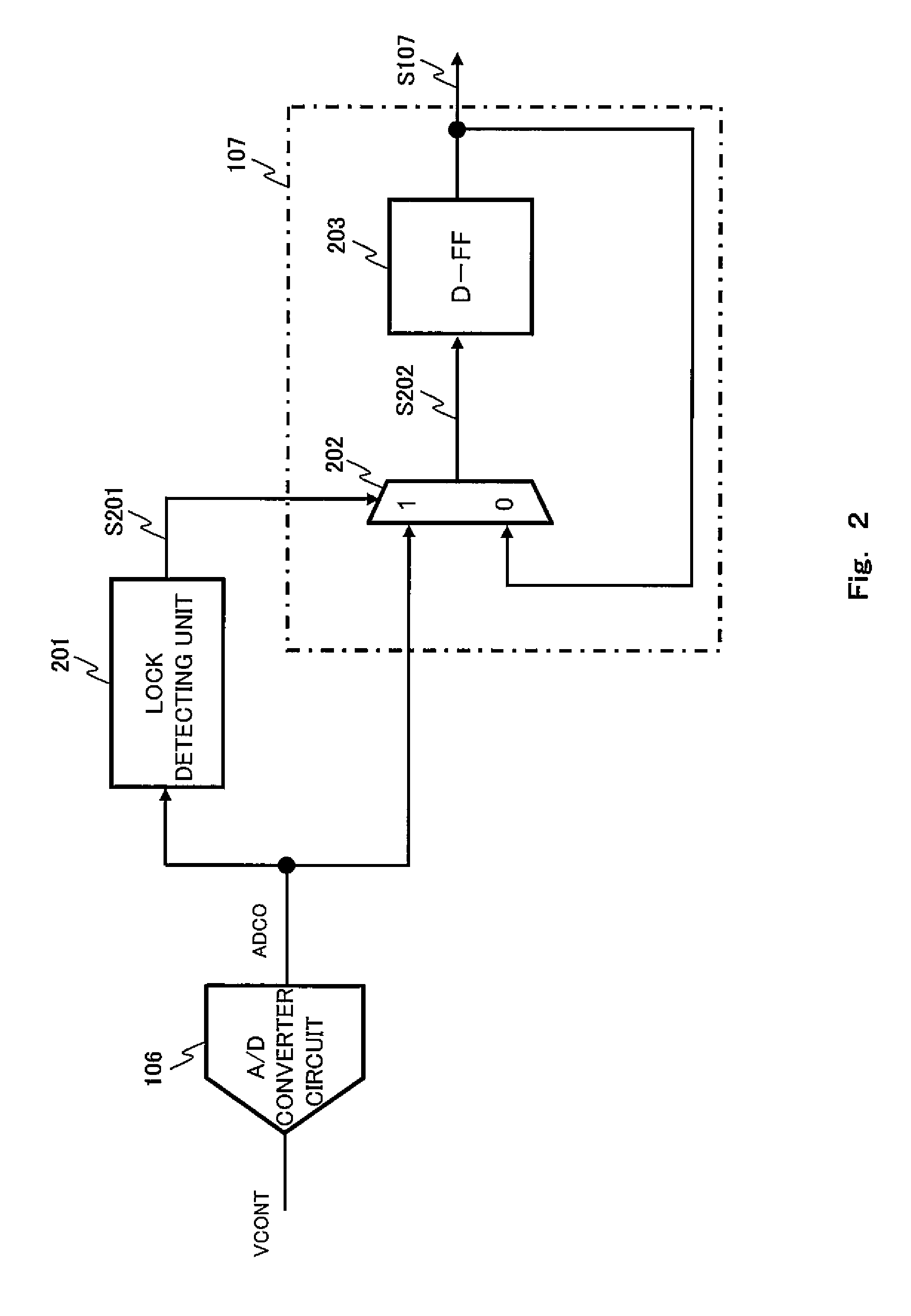
[0064]The configuration of the PLL circuit of Embodiment 3 (including the holding unit 107, and charge pump control unit 108) is identical to that of the PLL circuit of Embodiment 1 shown in FIG. 1, except that the holding unit 107 is adapted to hold an arbitrary digital signal ADCO rather than the lock digital signal ADCO in the first PLL operation. Since the holding unit 107 is implemented as a digital circuit, the value held in the holding unit 107 can be set as desired by a register, etc. With this configuration, an optimal timing when the charge pump current amount is reduced can be easily set.
PUM
 Abstract
Description
Claims
Application Information


