Liquid crystal display device implementing improved electrical lines and the fabricating method
a technology of liquid crystal display and electrical lines, applied in non-linear optics, instruments, optics, etc., can solve the problems of increasing material cost of lcd device, difficult to repair against drive ic or terminal lines troubles of lcd panel, and difficulty in installing drive ic on above-mentioned pcb, etc., to reduce the detectable brightness difference
- Summary
- Abstract
- Description
- Claims
- Application Information
AI Technical Summary
Benefits of technology
Problems solved by technology
Method used
Image
Examples
first preferred embodiment
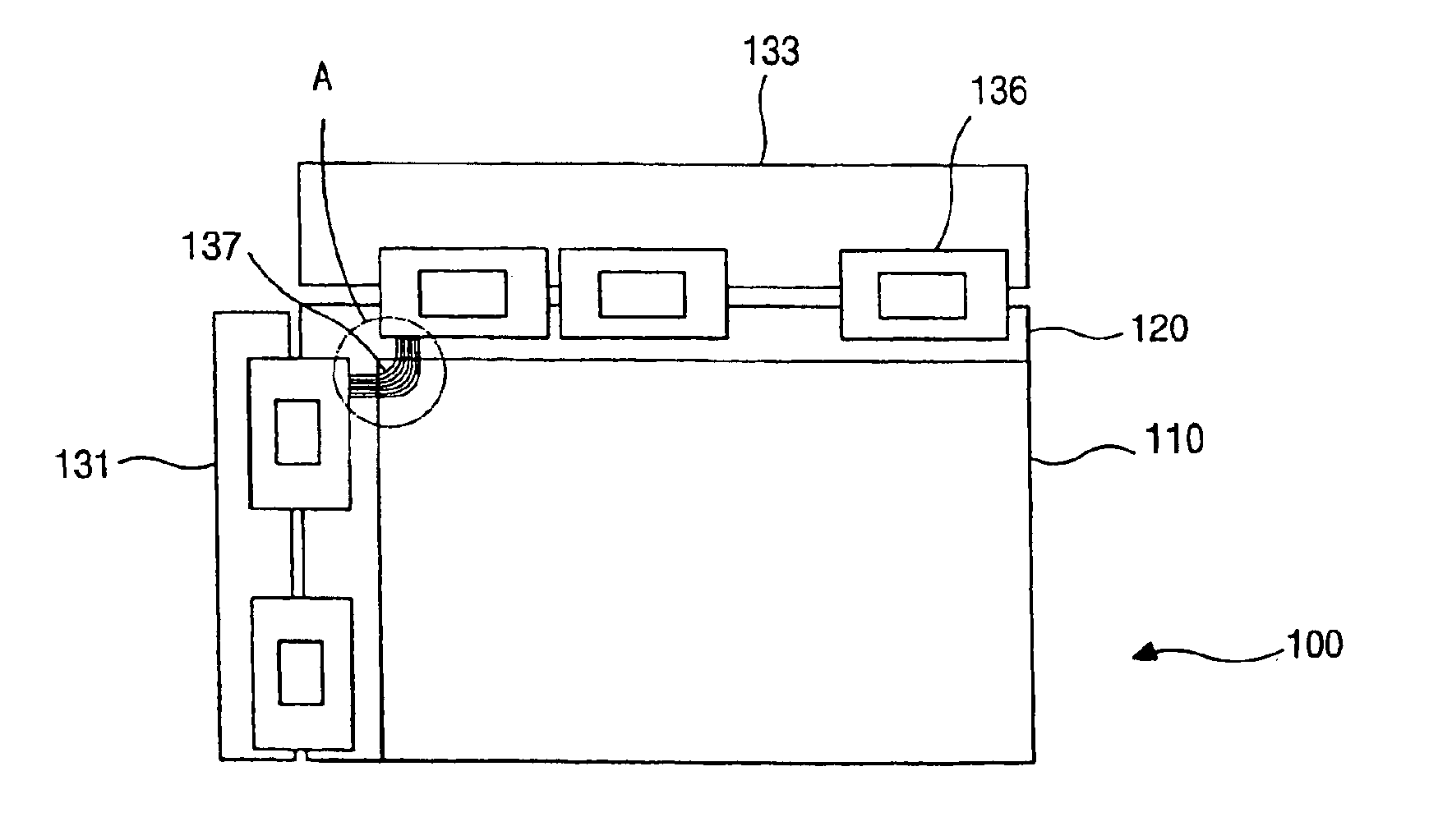
[0057]FIG. 5 is a plane view of a LCD device according to the first preferred embodiment of the present invention.
[0058]As shown, an upper substrate 110 is positioned over a lower substrate 120 with a liquid crystal (not shown) interposed between the upper and lower substrates 110 and 120. A sealant 141 shown in FIG. 6 is used to attach the lower and upper substrates 120 and 110. Around edges of the lower substrate 120, gate and source PCBs 131 and 133 are positioned. Gate and source TCPs 134 and 136 electrically connect, respectively, the gate and source PCBs 131 and 133 with a LCD panel 100 including the upper and lower substrates 110 and 120. A gate transmitting wires 137 electrically connects the gate TCP 134 with the source TCP 136 such that the source PCB 133 is electrically connected with the gate PCB 131. The gate transmitting wires 137 are preferably selected from a group consisting of aluminum (Al), molybdenum (Mo), chromium (Cr), alloys thereof and the like.
[0059]FIG. 6 i...
second preferred embodiment
[0065]The second preferred embodiment of the present invention provides a repair wire to repair a short line occurring in the gate transmitting wires provided by the first preferred embodiment of the present invention.
[0066]As shown in FIG. 8, over the gate transmitting wires 137, the repair wire 142 is formed with an insulating layer (not shown) interposed between the gate transmitting lines 137 and the repair wire 142. The repair wire 142 is inwardly spaced apart from the sealant 141 and overlaps two different portions of each gate transmitting wire 137. When a last gate transmitting wire 137a has a short line at a portion “E”, the repair wire 142 and the last gate transmitting wire 137a are welded together at their first and second cross points 145 and 147 using a laser and the like. By the above-mentioned repair, the voltage signal is transmitted again via the repair wire 142. The last gate transmitting wire 137a is only an example. When the other of the gate transmitting wires ...
third preferred embodiment
[0067]In a scribing and breaking process to separate at least two LCD panels independently from each other, a large sized upper substrate is scribed and broken by force into a plurality of the upper substrates 110 such that a plurality of the LCD panels are fabricated. The third preferred embodiment provides repair wires to repair the gate transmitting wires 137 that are broken in the above-mentioned scribing and breaking process.
[0068]Now, with reference to FIG. 9, the third preferred embodiment is explained.
[0069]As shown, adjacent to each gate pad 128 and each source pad 130, a gate dummy pad 157b and a source dummy pad 157a are formed respectively. Across the source pads 130 and the source dummy pads 157a, a first repair wire 150a is formed with an insulating layer (not shown) interposed between the pads and the repair wire. Similarly, a second repair wire 150b is formed across the gate pads 128 and the gate dummy pads 157a with the insulating layer interposed between the pads a...
PUM
| Property | Measurement | Unit |
|---|---|---|
| resistance | aaaaa | aaaaa |
| area | aaaaa | aaaaa |
| specific resistance | aaaaa | aaaaa |
Abstract
Description
Claims
Application Information


