Liquid crystal display device and method for fabricating the same

a liquid crystal display and display device technology, applied in non-linear optics, instruments, optics, etc., can solve the problems of serious degradation of image quality at the display area, inconvenient fabrication process of bottom substrate, and inability to use batch exposure techniques, etc., to reduce the detectable brightness difference

Inactive Publication Date: 2005-03-01
LG DISPLAY CO LTD
View PDF4 Cites 7 Cited by
  • Summary
  • Abstract
  • Description
  • Claims
  • Application Information

AI Technical Summary

Benefits of technology

It is therefore an object of the present invention to reduce the detectable difference in brightness resulting from the difference in distance between pixel electrodes and data lines at the boundaries of exposure regions for a liquid crystal display device having a larger display area.

Problems solved by technology

Recently, as the display area of the liquid crystal display device becomes larger, the fabricating process of the bottom substrate 2 becomes complicated.
Namely, in case of the bottom substrate of the liquid crystal display device having a larger than 10 inch-sized display area, the batch exposure technique is useless due to the diffraction of light incident from an exposure apparatus.
But, to fabricate the liquid crystal display device using the step-and-repeat exposure technique may give rise to a serious degradation of image quality at the display area.
Thus, no matter bow accurate exposure equipment and arrangement apparatus are used for the step-and-repeat exposure technique, it may give rise to misalignment between the exposure regions.
Since the exposure equipment or the arrangement apparatus has an accuracy limitation of itself, misalignment between the exposure regions may occur.
The misalignment may result in shift, rotation and distortion of the patterns, thereby causing defects such as disconnection of the wirings and differences in electrical properties between the exposure regions.

Method used


Image

  • Liquid crystal display device and method for fabricating the same
  • Liquid crystal display device and method for fabricating the same
  • Liquid crystal display device and method for fabricating the same

Examples


Embodiment Construction

Reference will now be made in detail to the preferred embodiment of the present invention, example of which is illustrated in the accompanying drawings.

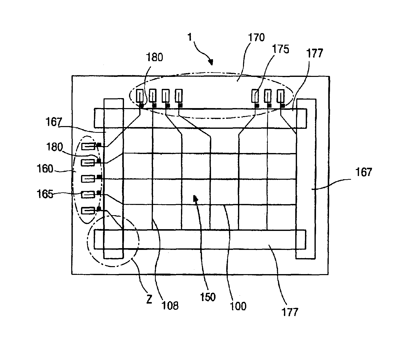
FIG. 5 is a partially expanded plan view illustrating a pixel of a liquid crystal display (LCD) device according to a preferred embodiment of the present invention.

For the sake of convenience in explanation, describing the construction of the pixel regardless of process orders, the pixel includes a gate line 100 arranged in a transverse direction, a data line 108 arranged in a longitudinal direction perpendicular to the gate line 100, pixel electrodes 114 disposed between a pair of the data lines 108 and the gate line 100, and a thin film transistor (TFT) arranged near the cross point of the gate and data lines 100 and 108. The TFT includes a gate electrode 106, a source electrode 110 and a drain electrode 112.

The gate line 100 includes a gate electrode 106, and light shielding portions 102 perpendicularly extended upward and downwar...


PUM

PropertyMeasurementUnit
temperatureaaaaaaaaaa
widthaaaaaaaaaa
temperatureaaaaaaaaaa

Abstract

The present invention discloses a method of manufacturing a liquid crystal display device, including depositing a first metal layer on a transparent substrate; patterning the metal layer to form a gate line, the gate line having a gate electrode portion; depositing sequentially an insulating layer, an amorphous silicon layer and a doped amorphous silicon layer on the exposed surface of the transparent substrate while covering the gate line; patterning the amorphous silicon layer and the doped amorphous silicon layer to form a semiconductor island; depositing a second metal layer on the exposed surface of the insulating layer while covering the semiconductor island; patterning the second metal layer to form a source electrode, a drain electrode, and a capacitor electrode, the drain electrode spaced apart from the source electrode; etching the doped amorphous silicon layer of the semiconductor island to from an active area; forming a passivation film over the whole surface of the substrate while covering the source electrode, the drain electrode and the capacitor electrode; depositing a transparent conductive material layer on the passivation film; applying a negative photoresist on the transparent conductive material layer; performing a back side exposure to form a first exposed portion of the negative photoresist; aligning a patterning mask with the negative photoresist; performing a front side exposure to form a second exposed portion of the negative photoresist, the second exposed portion overlapping the first exposed portion; baking the transparent conductive material layer; and patterning the transparent conductive material layer to form a pixel electrode.

Description

CROSS REFERENCEThis application claims the benefit of Korean Patent Application No. 1999-31487, filed on Jul. 31, 1999, under 35 U.S.C. § 119, the entirety of which is hereby incorporated by reference.BACKGROUND OF THE INVENTION1. Field of the InventionThe present invention relates to a liquid crystal display (LCD) device, and more particularly, to a liquid crystal display device having a thin film transistor (TFT) and a method of manufacturing the same.2. Description of Related ArtA typical liquid crystal display device uses optical anisotropy and polarization properties of liquid crystal molecules. The liquid crystal molecules have a definite orientational order in arrangement resulting from their thin and long shapes. The arrangement direction of the liquid crystal molecules can be controlled by supplying an electric field to the liquid crystal molecules. In other words, as the arrangement direction of the liquid crystal molecules is changed, the arrangement of the liquid crystal...

Claims


Application Information

Patent Timeline
Patent Type & Authority Patents(United States)
IPC IPC(8): G02F1/13G02F1/1362G02F1/136
CPCG02F1/1362G02F2001/136295G02F2001/136231G02F1/136209G02F1/136231G02F1/136295G02F1/136
Inventor PARK, DUG-JIN
Owner LG DISPLAY CO LTD
Why Eureka
Try Eureka