Method for forming an asymmetric crystalline structure memory cell

a technology of crystalline structure and memory cell, which is applied in the direction of digital storage, nanomagnetism, instruments, etc., can solve the problems of device more susceptible to process tolerance errors, change in cmr resistance, and inapplicability to dense memory array applications

Inactive Publication Date: 2005-08-09
SAMSUNG ELECTRONICS CO LTD
View PDF3 Cites 27 Cited by
  • Summary
  • Abstract
  • Description
  • Claims
  • Application Information

AI Technical Summary

Benefits of technology

This patent introduces a new type of memory chip that uses a special material called an asymmetric crystal. It has been found that this material allows for reliable programming of the chip's cells, regardless of their tiny size or symmetrical design. The technical effect of this innovation is better performance and efficiency of the memory chip, making it more robust against errors and faster than previous versions.

Problems solved by technology

The technical problem addressed in this patent text is how to design a memory resistor memory cell that can be properly programmed and erased despite its geometric symmetry. This is challenging because smaller feature sizes make the device more susceptible to process tolerance errors, which can result in a low net resistance change from high to low. The invention aims to address this problem by designing features in the memory cell that can ensure proper programming and erasing operations.

Method used


Image

  • Method for forming an asymmetric crystalline structure memory cell
  • Method for forming an asymmetric crystalline structure memory cell
  • Method for forming an asymmetric crystalline structure memory cell

Examples


Embodiment Construction

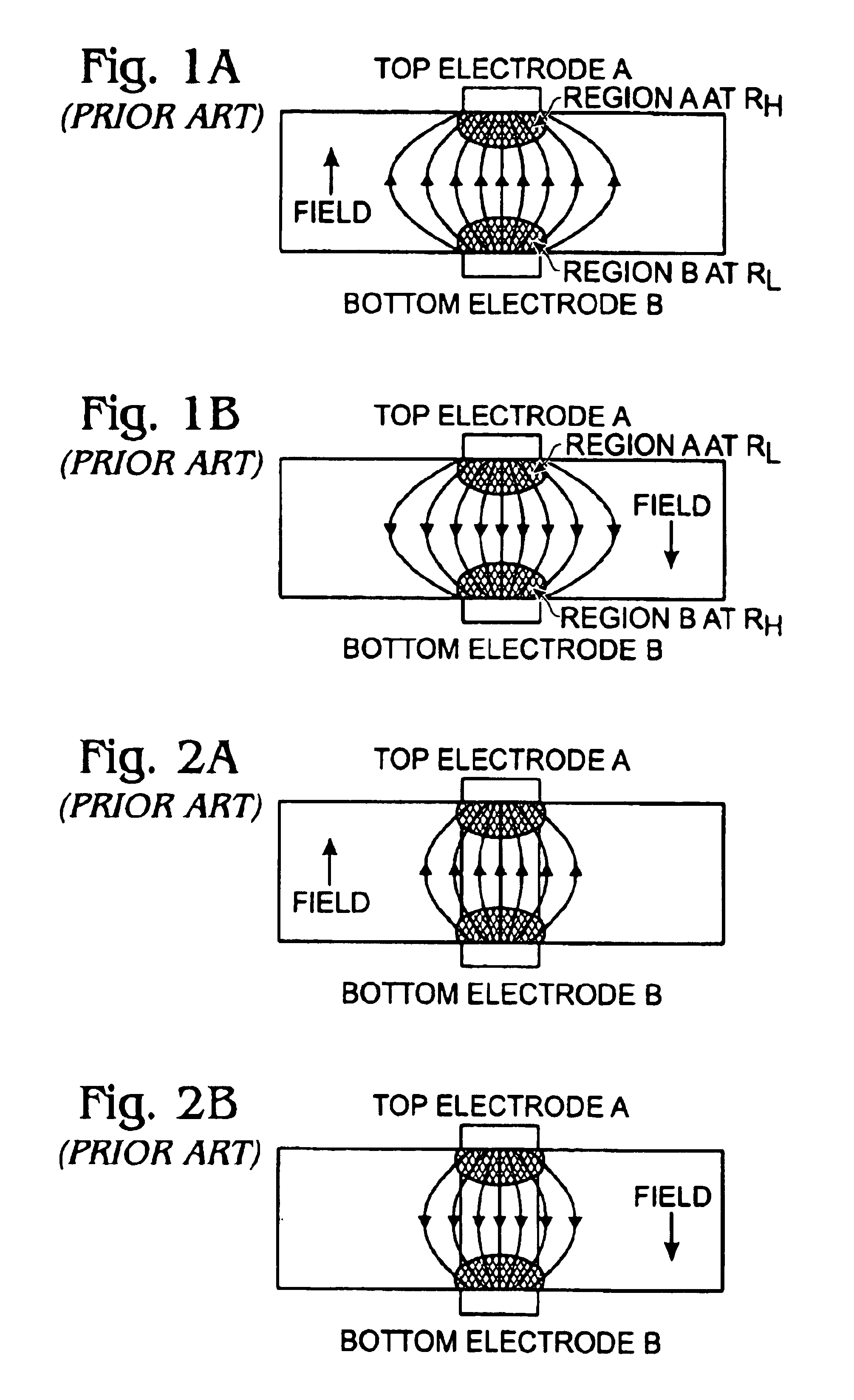
[0019]FIGS. 1A and 1B are partial cross-sectional views of a memory cell during programming (FIG. 1A) and erasing (FIG. 1B) operations. The top and bottom electrodes are identical and the memory resistance material is uniform throughout. If the geometric structure of the device could be made perfectly symmetrical, the net resistance would remains constant, in a high-resistance state, when either a negative field (FIG. 1A) or a positive field (FIG. 1B) is applied. Note that the electric fields are defined with respect to the top electrode. That is, the fields are induced at the top electrode. In such circumstances, programming is not possible. Therefore, a geometrically symmetrical device structure, such as one in FIGS. 1A and 1B, is not practical.

[0020]More specifically, the geometrically symmetric memory cell has a high current density near the electrodes (regions A and B), and a low current density in the center portion of the device, in the presence of an electric field. As a res...


PUM


Abstract

Asymmetrically structured memory cells and a fabrication method are provided. The method comprises: forming a bottom electrode; forming an electrical pulse various resistance (EPVR) first layer having a polycrystalline structure over the bottom electrode; forming an EPVR second layer adjacent the first layer, with a nano-crystalline or amorphous structure; and, forming a top electrode overlying the first and second EPVR layers. EPVR materials include CMR, high temperature super conductor (HTSC), or perovskite metal oxide materials. In one aspect, the EPVR first layer is deposited with a metalorganic spin coat (MOD) process at a temperature in the range between 550 and 700 degrees C. The EPVR second layer is formed at a temperature less than, or equal to the deposition temperature of the first layer. After a step of removing solvents, the MOD deposited EPVR second layer is formed at a temperature less than, or equal to the 550 degrees C.

Description


Claims


Application Information

Patent Timeline
Owner SAMSUNG ELECTRONICS CO LTD
Why Eureka
Try Eureka