One-time programmable device having an LDMOS structure

a one-time programmable, semiconductor technology, applied in semiconductor devices, basic electric elements, instruments, etc., can solve the problems of high manufacturing cost low manufacturing efficiency, and low manufacturing efficiency of conventional otp devices

Active Publication Date: 2013-07-23
AVAGO TECH INT SALES PTE LTD
View PDF4 Cites 0 Cited by
  • Summary
  • Abstract
  • Description
  • Claims
  • Application Information

AI Technical Summary

Benefits of technology

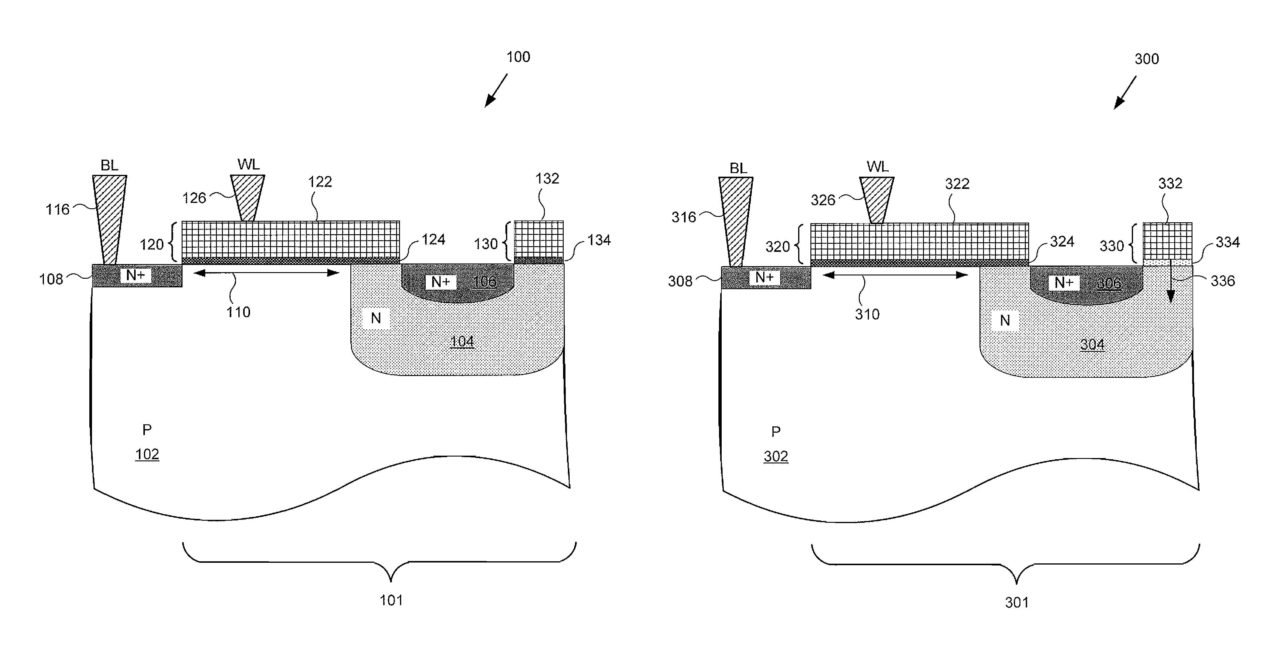
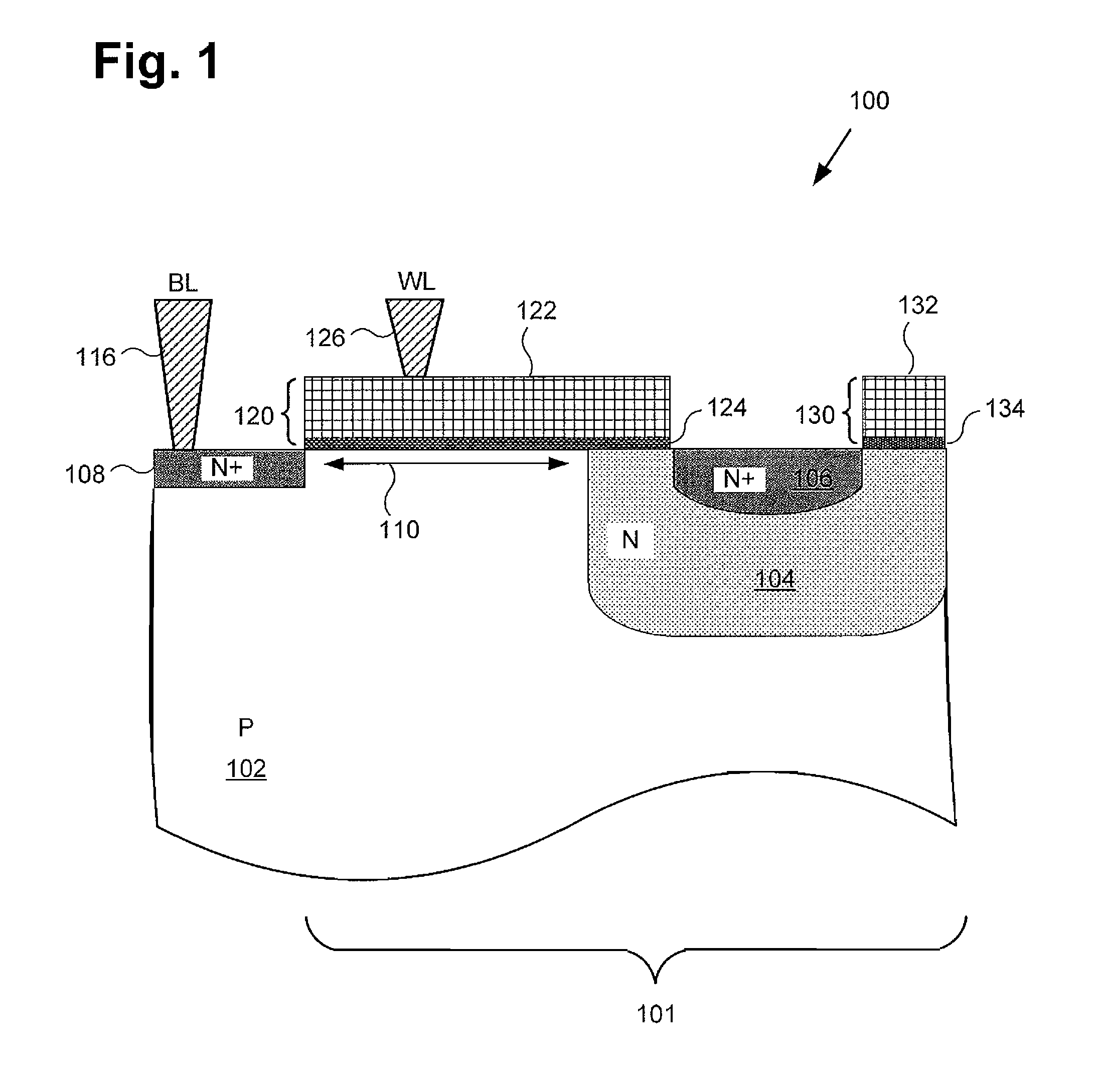
[0028]Thus, the structures and methods according to the present invention enable several advantages over the conventional art. For example, by adopting an LDMOS structure, embodiments of the OTP device disclosed by the present application are configured to withstand higher programming voltages than would otherwise be the case, thereby rendering programming more reliable while advantageously providing enhanced protection for a pass gate portion of the OTP device. In addition, a programming gate of embodiments of the disclosed OTP device may be fabricated using a high-κ metal gate process, such that, after programming, a Schottky contact is formed between a programming gate electrode and a drain region of the OTP device, thereby enabling improved conduction in a forward biased state. Moreover, the advantages associated with this approach can be realized using existing high-κ metal gate CMOS process flows, making integration of high voltage devices and CMOS core and IO devices on a common IC efficient and cost effective. As a result, the present invention improves design flexibility without adding cost or complexity to established semiconductor device fabrication processes.

Problems solved by technology

Although this functionality is in great demand, conventional OTP elements (the programmable constituent of an OTP device) can be larger than desired or can require multiple additional fabrication steps beyond those required for conventional transistor fabrication, for example, making conventional OTP devices expensive to manufacture and embed.
This approach, however, has a relatively high tendency to result in devices with programmed states where the remaining thick gate structure exhibits a high leakage current due to collateral damage during programming.
In addition, this approach tends to render devices with relatively poorly differentiated programmed and un-programmed states (as seen by a sensing circuit), which, in combination with the high leakage current statistics, require a relatively high voltage sensing circuit to reliably read out programmed and un-programmed states.
Mitigation of these shortcomings can require additional die space for high-voltage sensing circuitry and / or for redundancy techniques, for example, which can involve undesirable increases in manufacturing cost.

Method used


Image

  • One-time programmable device having an LDMOS structure
  • One-time programmable device having an LDMOS structure
  • One-time programmable device having an LDMOS structure

Examples


Embodiment Construction

[0012]The present invention is directed to a one-time programmable (OTP) device having a lateral diffused metal-oxide-semiconductor (LDMOS) structure and related method. The following description contains specific information pertaining to the implementation of the present invention. One skilled in the art will recognize that the present invention may be implemented in a manner different from that specifically discussed in the present application. Moreover, some of the specific details of the invention are not discussed in order not to obscure the invention.

[0013]The drawings in the present application and their accompanying detailed description are directed to merely exemplary embodiments of the invention. To maintain brevity, other embodiments of the present invention are not specifically described in the present application and are not specifically illustrated by the present drawings. It should be understood that unless noted otherwise, like or corresponding elements among the fi...


PUM


Abstract

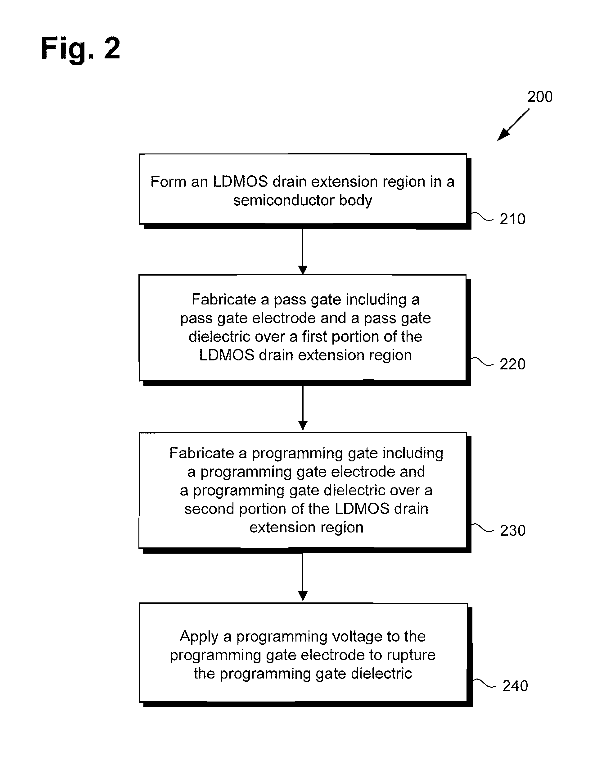
According to one embodiment, a one-time programmable (OTP) device having a lateral diffused metal-oxide-semiconductor (LDMOS) structure comprises a pass gate including a pass gate electrode and a pass gate dielectric, and a programming gate including a programming gate electrode and a programming gate dielectric. The programming gate is spaced from the pass gate by a drain extension region of the LDMOS structure. The LDMOS structure provides protection for the pass gate when a programming voltage for rupturing the programming gate dielectric is applied to the programming gate electrode. A method for producing such an OTP device comprises forming a drain extension region, fabricating a pass gate over a first portion of the drain extension region, and fabricating a programming gate over a second portion of the drain extension region.

Description

BACKGROUND OF THE INVENTION[0001]1. Field of the Invention[0002]The present invention is generally in the field of semiconductors. More particularly, the present invention is in the field of one-time programmable semiconductor devices.[0003]2. Background Art[0004]One-time programmable (OTP) devices are used throughout the semiconductor industry to allow for post-fabrication design changes in integrated circuits (ICs). For example, after post-fabrication functionality testing but before sale to a customer, a semiconductor device manufacturer can program a network of OTP devices embedded in a particular semiconductor die to provide a permanent serial number encoding for that particular die. Under other circumstances, a single OTP device can be programmed to permanently enable or disable a portion of an integrated circuit at any time after fabrication, including after sale to a customer. Although this functionality is in great demand, conventional OTP elements (the programmable constit...

Claims


Application Information

Patent Timeline
Patent Type & Authority Patents(United States)
IPC IPC(8): G11C17/00H01L23/52
CPCH01L27/11206H01L23/5252H01L27/088H01L29/7816H01L29/66681H01L21/76224H01L29/495H01L29/4966H01L2924/0002H01L29/517H01L29/7835H01L27/11226H01L27/1124H01L27/11246H01L27/11266H01L2924/00H10B20/34H10B20/363H10B20/20H10B20/367H10B20/387
Inventor ITO, AKIRACHEN, XIANGDONG
Owner AVAGO TECH INT SALES PTE LTD
Why Eureka
Try Eureka