Encapsulation of organic electronic devices using adsorbent loaded adhesives
a technology of organic electronic devices and adhesives, which is applied in the direction of discharge tubes luminescnet screens, other domestic articles, etc., can solve the problems of light, oxygen, moisture, and heat adversely affecting many inorganic materials, and achieve the effect of simplifying the encapsulation process and enhancing the ability to prevent moisture and/or oxygen induced oed degradation
- Summary
- Abstract
- Description
- Claims
- Application Information
AI Technical Summary
Benefits of technology
Problems solved by technology
Method used
Image
Examples
example 1
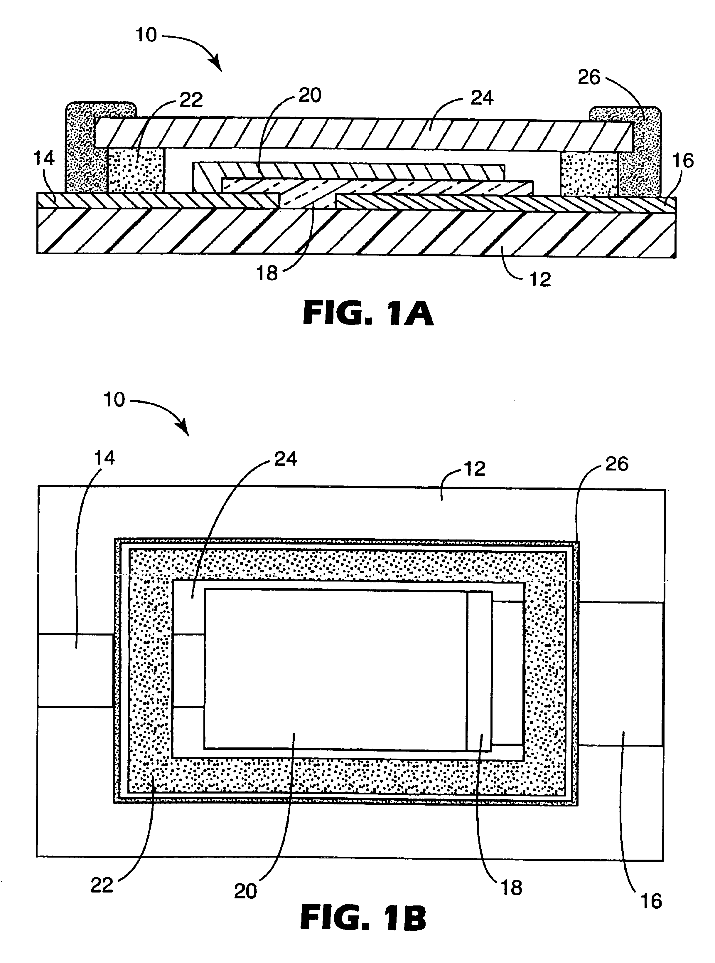
[0043]This example describes the making of an OLED with a gasket-like adsorbent-loaded adhesive layer. FIG. 1 is an illustration of an OLED device made as described in this example.
[0044]A 2″×3″ indium tin oxide (ITO), coated glass slide, available from Thin Film Devices, Long Beach, Calif., was etched to form a simple pattern of two ITO pads (electrodes) with a small (1-3 mm) gap in between. The etching took place in a heated hydrochloric acid bath (about 60° C.) and the masking was accomplished using a commercially available plating tape. Following completion of the etching, the tape was removed and the unetched portion of the ITO on glass was cleaned using a methanol rub and oxygen plasma exposure. A thin film of poly(ethylenedioxythiophene) (PEDOT) (available as product number 4083 from Bayer, Pittsburgh, Pa.) was deposited on the surface by spin coating (not shown in FIG. 1). The PEDOT coated ITO on glass was baked on a hotplate at about 100° C. for about 5-10 minutes.
[0045]Aft...
example 2
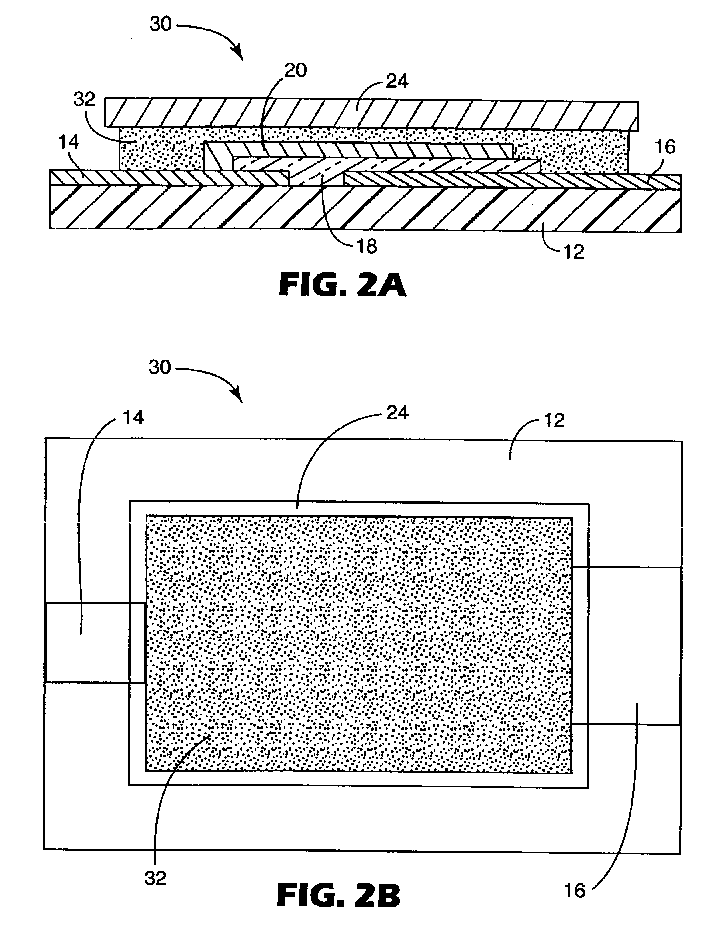
[0050]This example describes the making of an OLED with a continuous adsorbent-loaded adhesive layer. FIG. 2 is an illustration of an OLED device made as described in this example.
[0051]An unencapsulated OLED device was made in the same manner as described in Example 1. Also as in Example 1, upon completion of the thin film stack deposition the sample was removed from the vacuum system and immediately introduced into a nitrogen glove box. A thin (0.2 mm) glass slide was used as the encapsulating lid. It was placed on a hotplate in the nitrogen glove box and heated to about 130° C.
[0052]A rectangular piece of the dessicant loaded hotmelt adhesive film of Example 1 was cut out with scissors to fit directly over (and almost entirely cover) the thin glass encapsulating lid. The resulting adhesive piece was placed on top of the hot encapsulating lid, began to soften and develop a wet appearance after about 3-5 minutes. Following this change, the OLED lamp was placed cathode side down ont...
PUM
| Property | Measurement | Unit |
|---|---|---|
| width | aaaaa | aaaaa |
| width | aaaaa | aaaaa |
| width | aaaaa | aaaaa |
Abstract
Description
Claims
Application Information

