Deuterium incorporated nitride

a nitride and deuterium technology, applied in the field of deuterium incorporated nitride, can solve the problems of reduced channel conductance, transistor performance degradation, and non-ideal capacitance-voltage characteristics

Inactive Publication Date: 2005-09-13
INFINEON TECH LLC
View PDF16 Cites 33 Cited by
  • Summary
  • Abstract
  • Description
  • Claims
  • Application Information

AI Technical Summary

Benefits of technology

[0010]The phrase “deuterium enriched” means that the amount of deuterium, as a percent of the hydrogen present, is greater than the amount that would be expected based on the natural isotopic abundance of deuterium in hydrogen. Preferably, at least 90% of the hydrogen is deuterium, more preferably at least 99%.

Problems solved by technology

Dangling bonds at the silicon / silicon oxide interface in semiconductor devices are believed to be the cause of observed non-ideal capacitance-voltage characteristics and reduced channel conductance.
During operation, however, transistor performance can degrade, and this degradation has been correlated to the removal of hydrogen from the silicon / silicon oxide interface, due to collisions between heated carriers and the interface.
This degradation in hot carrier lifetime (also referred to as HCl lifetime) is exacerbated by the ever ongoing miniaturization of semiconductor devices, and has become a significant limitation in the further shrinkage of semiconductor devices.
Continued miniaturization is severely limiting the usefulness of these techniques.
It has been discovered, however, that deuterium is unable to penetrate through silicon nitride layers, present in many semiconductor devices as etch-stop layers and gate spacers.
If the deuterium annealing is carried out prior to the formation of the silicon nitride layers, the high-temperatures necessary to form the silicon nitride layers, as well as the boron-phosphorous spin glass layers conventionally used as interlayer dielectrics (formed at 750° C. or more), may cause the deuterium to diffuse out.
Attempts to overcome these problems have relied on expensive techniques, such as using deuterated silane and ammonia to form the silicon nitride layers, or dangerous techniques, such as annealing in a 100% deuterium atmosphere.

Method used


Image

  • Deuterium incorporated nitride
  • Deuterium incorporated nitride
  • Deuterium incorporated nitride

Examples


example

Example 1

Formation of a Gate Structure

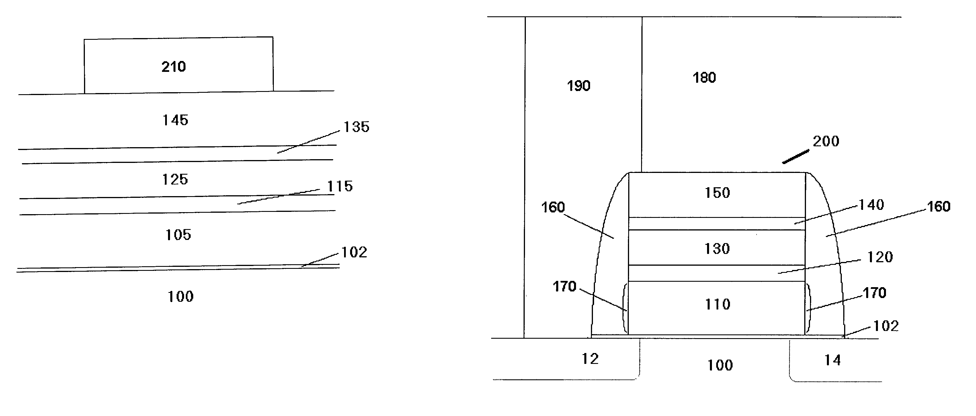
[0042]The following detailed steps would be used to form the gate stack having a split gate:

[0043]

Nitrogen-containing gate oxide formationPoly deposition - single amorphous gate depositMask for P-dopingP+ poly implantationN-well implantationP-channel implantationP+ poly implantation strip resistMask for N-dopingP-well implantationN+ poly implantationN-channel implantationN+ poly implantation strip resistTungsten gate pre-cleanTungsten PVD, sputtering (nitrogen + argon, thenargon only)Nitride - ND3 and BTBASDeposit ARC and ResistEtch mask for nitrideNitride etch - ARC, silicon nitride, and partialtungsten etchRemove resistTungsten and Poly etchPost-poly etch cleanSelective oxidationN+ source / drain extension implantStripping & cleaningP+ source / drain extension implantStripping & cleaningNitride spacer deposition (BTBAS chemistry)Spacer etchPost-spacer etch cleanN+ source / drain implantStripping & cleaningP+ source / drain implantStripping & cleaningN...


PUM


Abstract

A method of forming a semiconductor structure comprises forming an etch-stop layer comprising nitride, on a stack. The stack is on a semiconductor substrate, and the stack comprises (i) a gate layer. The forming is by CVD with a gas comprising a first compound which is SixL2x, and a second compound comprising nitrogen and deuterium, L is an amino group, and X is 1 or 2.

Description

BACKGROUND[0001]The present invention relates to semiconductor structures, semiconductor devices and methods of making the same.[0002]Dangling bonds at the silicon / silicon oxide interface in semiconductor devices are believed to be the cause of observed non-ideal capacitance-voltage characteristics and reduced channel conductance. Low temperature post-metallization annealing in a hydrogen-containing atmosphere is typically used in the semiconductor device fabrication process, to passivate these dangling bonds. During operation, however, transistor performance can degrade, and this degradation has been correlated to the removal of hydrogen from the silicon / silicon oxide interface, due to collisions between heated carriers and the interface. This degradation in hot carrier lifetime (also referred to as HCl lifetime) is exacerbated by the ever ongoing miniaturization of semiconductor devices, and has become a significant limitation in the further shrinkage of semiconductor devices.[000...

Claims


Application Information

Patent Timeline
Patent Type & Authority Patents(United States)
IPC IPC(8): H01L21/02H01L21/469H01L21/31
CPCH01L21/02063H01L21/02071H01L21/0217H01L21/02219H01L21/02271H01L21/28176H01L21/31116H01L21/31138H01L21/32139H01L21/76834H01L29/518
Inventor NARAYANAN, SUNDARRAMKUMAR, KRISHNASWAMY
Owner INFINEON TECH LLC
Why Eureka
Try Eureka