Temporary semiconductor structure bonding methods and related bonded semiconductor structures

a technology of bonded semiconductors and semiconductor structures, applied in semiconductor devices, semiconductor/solid-state device details, electrical devices, etc., can solve problems such as limiting the temperature at which semiconductor device fabrication may be conducted, prone to cracking, fracture or other damage, and unstable adhesive materials

Active Publication Date: 2012-01-19
S O I TEC SILICON ON INSULATOR THECHNOLOGIES
View PDF2 Cites 258 Cited by
  • Summary
  • Abstract
  • Description
  • Claims
  • Application Information

AI Technical Summary

Problems solved by technology

However, the benefits that may be produced by thinning of the one or more semiconductor structure comprising the 3D integrated semiconductor structure may also introduce process complications, for example, a semiconductor structure may become relatively brittle due to a thinning process and may, thus, be susceptible to cracking, fracture or other damage during processing using existing equipment and materials.
Adhesive materials may be unstable at increased temperatures, however, which may limit the temperatures at which semiconductor device fabrication may be conducted.
This

Method used


Image

  • Temporary semiconductor structure bonding methods and related bonded semiconductor structures
  • Temporary semiconductor structure bonding methods and related bonded semiconductor structures
  • Temporary semiconductor structure bonding methods and related bonded semiconductor structures

Examples


embodiment 1

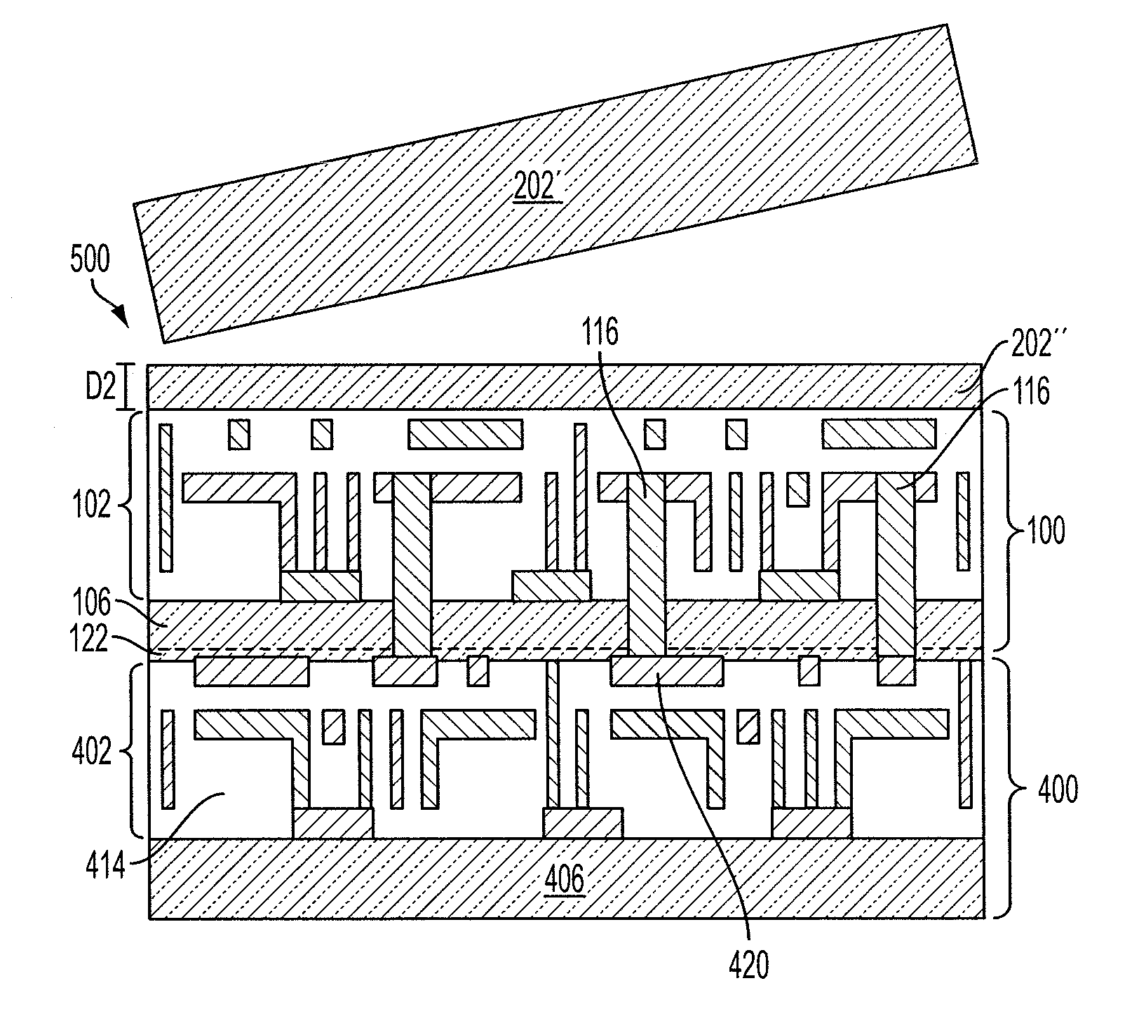
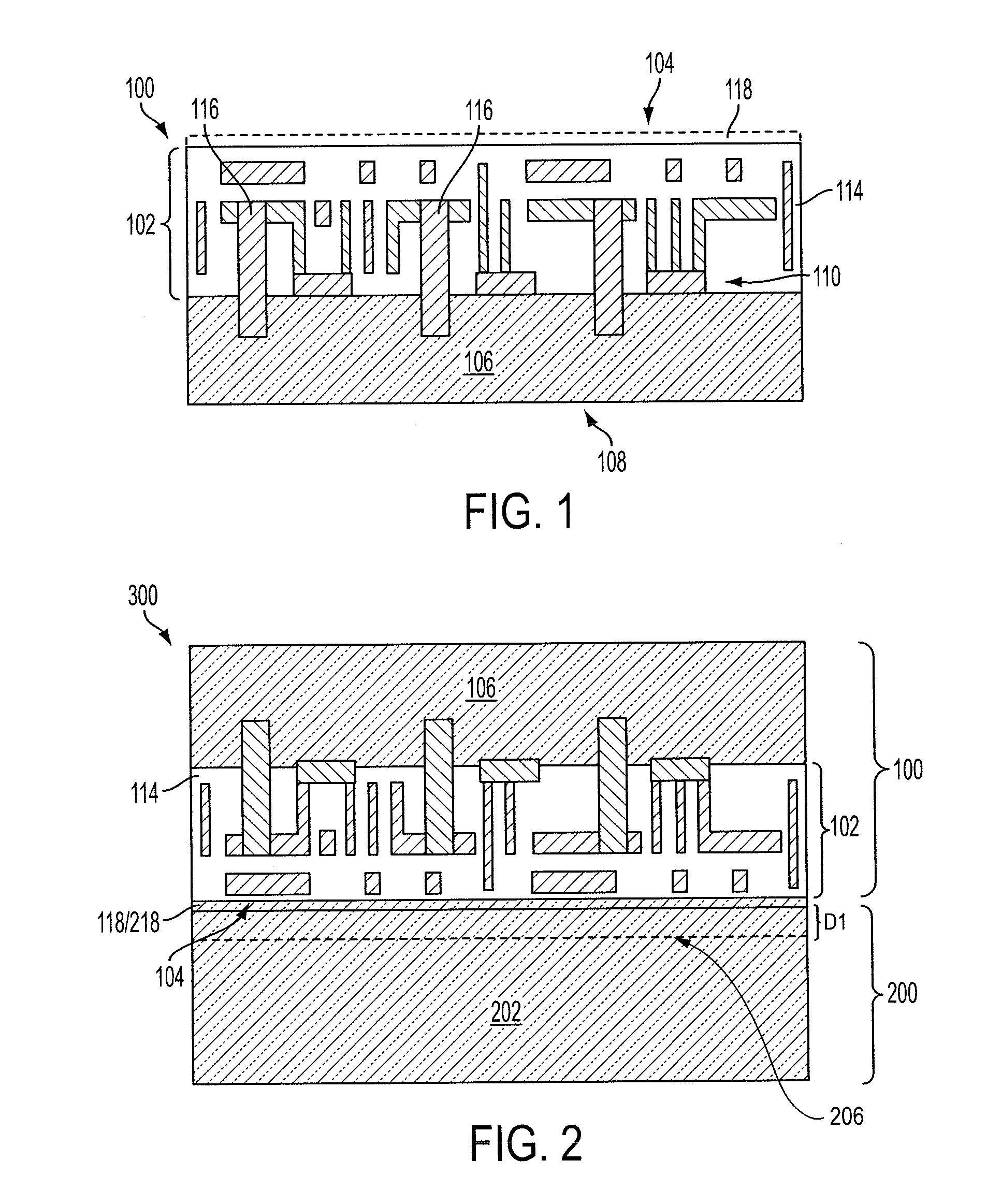
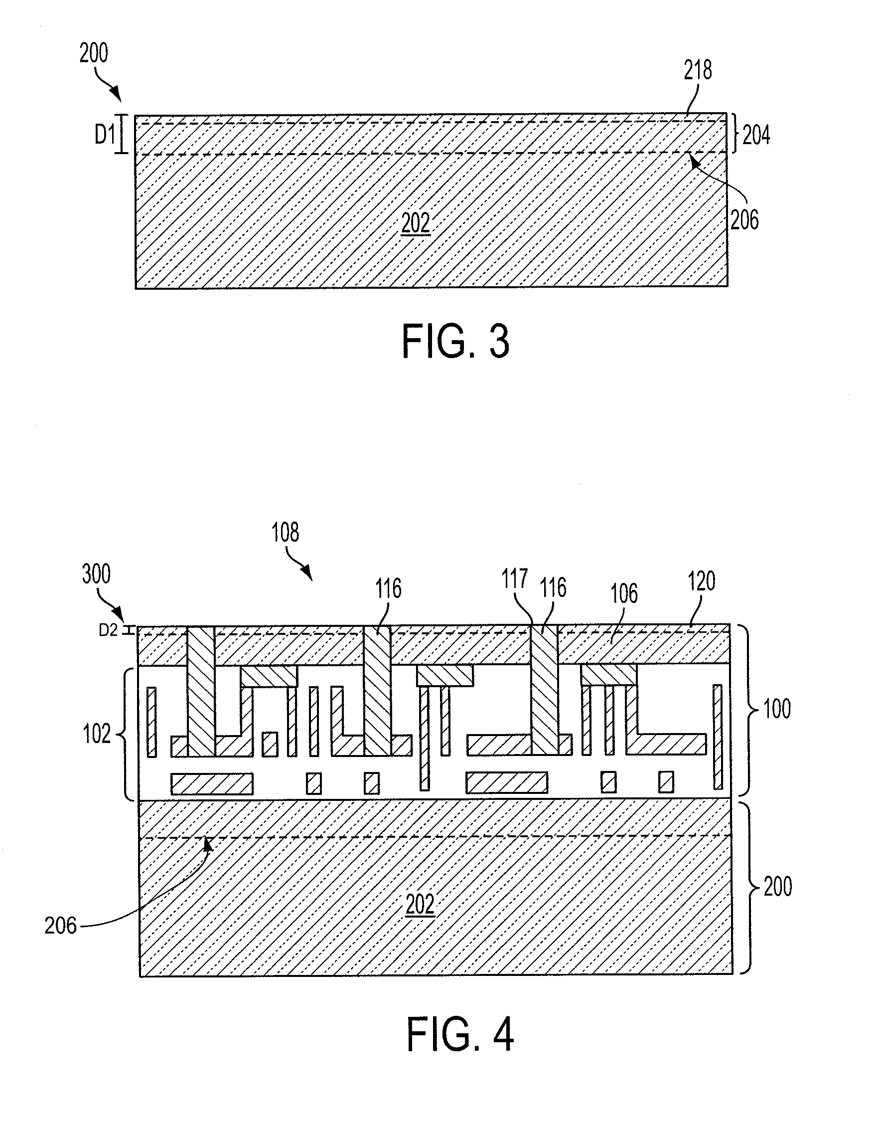
[0067]A method of fabricating a semiconductor structure, comprising: forming a first semiconductor structure including at least a portion of an integrated circuit on a first substrate; implanting ions into a carrier wafer to form a weakened region within the carrier wafer; directly bonding the carrier wafer to a first side of the first semiconductor structure; processing the first semiconductor structure while the carrier wafer is attached to the first semiconductor using the carrier wafer to handle the first semiconductor structure; directly bonding a second semiconductor structure including at least a portion of an integrated circuit to a second side of the first semiconductor structure opposite the first side of the semiconductor structure to which the carrier wafer is directly bonded; and separating a layer of material from the carrier wafer from a remaining portion of the carrier wafer along the weakened region therein.

embodiment 2

[0068]The method of Embodiment 1, further comprising forming at least one through wafer interconnect (TWI) extending at least partially through the first substrate.

embodiment 3

[0069]The method of Embodiment 1 or Embodiment 2, wherein processing the first semiconductor structure comprises removing a portion of the first substrate from the second side of the first semiconductor structure and exposing at least one conductive structure of the at least a portion of the integrated circuit of the first semiconductor structure.


PUM


Abstract

Methods of fabricating semiconductor structures include implanting atom species into a carrier die or wafer to form a weakened region within the carrier die or wafer, and bonding the carrier die or wafer to a semiconductor structure. The semiconductor structure may be processed while using the carrier die or wafer to handle the semiconductor structure. The semiconductor structure may be bonded to another semiconductor structure, and the carrier die or wafer may be divided along the weakened region therein. Bonded semiconductor structures are fabricated using such methods.

Description

TECHNICAL FIELD[0001]The present invention generally relates to temporary semiconductor die and / or wafer bonding methods useful in forming three-dimensional semiconductor structures, to intermediate structures formed using the temporary semiconductor die and / or wafer bonding methods, and to semiconductor dice and / or wafers including an ion implanted zone for use in temporary semiconductor wafer bonding methods.BACKGROUND[0002]The three-dimensional (3D) integration of two or more semiconductor structures can produce a number of benefits to microelectronic applications. For example, 3D integration of microelectronic components can result in improved electrical performance and power consumption while reducing the area of the device foot print. See, for example, P. Garrou, et al. “The Handbook of 3D Integration,” Wiley-VCH (2008).[0003]The 3D integration of semiconductor structures may take place by the attachment of a semiconductor die to one or more additional semiconductor dies (i.e....

Claims


Application Information

Patent Timeline
IPC IPC(8): H01L23/52H01L21/30
CPCH01L2924/01322H01L2224/16145H01L2224/73204H01L23/5384H01L23/562H01L2924/10253H01L2224/80357H01L2224/0903H01L2224/0401H01L2924/13091H01L2924/1301H01L2924/1305H01L21/2007H01L21/6835H01L21/76898H01L24/03H01L24/05H01L24/08H01L24/27H01L24/29H01L24/32H01L24/80H01L24/83H01L24/92H01L24/94H01L25/50H01L2221/68327H01L2221/68363H01L2221/68377H01L2221/68381H01L2224/03616H01L2224/0362H01L2224/04026H01L2224/05009H01L2224/056H01L2224/05647H01L2224/05687H01L2224/08146H01L2224/27444H01L2224/27616H01L2224/29187H01L2224/32145H01L2224/80006H01L2224/80011H01L2224/80121H01L2224/802H01L2224/80203H01L2224/80805H01L2224/80895H01L2224/80896H01L2224/80905H01L2224/83005H01L2224/83011H01L2224/83022H01L2224/83121H01L2224/83191H01L2224/83193H01L2224/832H01L2224/83203H01L2224/83805H01L2224/83896H01L2224/92H01L2224/9211H01L2224/94H01L2225/06513H01L2225/06541H01L2924/01013H01L2924/01029H01L2924/01051H01L2924/01079H01L2924/01005H01L2924/01006H01L2924/01019H01L2924/01023H01L2924/01033H01L2924/01074H01L2224/80H01L2224/83H01L2924/00014H01L2924/05042H01L2924/05442H01L2924/00H01L2924/3512H01L2224/08121H01L2224/83205H01L2924/12042H01L2924/14H01L2224/80894H01L2924/00012H01L21/76254H01L24/28H01L24/98
Inventor SADAKA, MARIAMRADU, IONUT
Owner S O I TEC SILICON ON INSULATOR THECHNOLOGIES
Why Eureka
Try Eureka