Floating-gate memory cell having trench structure with ballistic-charge injector, and the array of memory cells

a memory cell and trench structure technology, applied in the field of nonvolatile memory, can solve the problems of complex process technology for nonvolatile memories, voltage infrastructure, and the scalability of new generation technologies, and achieve the effects of improving eprom and eeprom memory cells, improving manufacturability, and large topography in cell structures

Inactive Publication Date: 2005-10-25
MARVELL ASIA PTE LTD
View PDF9 Cites 82 Cited by
  • Summary
  • Abstract
  • Description
  • Claims
  • Application Information

AI Technical Summary

Benefits of technology

[0010]The present invention solves the aforementioned problems by providing improvements on EPROM and EEPROM memory cell. Specifically on cell architecture and fabrication method for compact cell size, as well as on cell operation method enabling memory cells for extended applications without needs on high voltage. Additionally, the present invention does not require stringent control on trench depth as observed in U.S. Pat. No. 5,146,426 nor involve a large topography in cell structure as observed in U.S. Pat. Nos. 5,432,739 and 5,563,083. The present invention therefore further provides advantages on better manufacturability over prior inventions.

Problems solved by technology

Therefore, it complicates process technology for nonvolatile memories.
Another issue on the high voltage infrastructure is its scalability along new generation technology.
The high voltage is found un-scalable or difficult to be scaled due to the physics employed in memory cell operation.
As a result, a larger overhead, in terms of the area occupied by high voltage circuitry, is often seen in newer generation memory products (in both stand-alone and embedded nonvolatile memory products).
The scaling limit on high voltage further imposes constraints on the scaling of the minimum feature size for high-voltage transistors.
Furthermore the high voltage operation introduces more issues in product functionality and reliability area.
However, the mechanisms thus involved require high voltages to support the operation.
It is believed that the high voltage demands stringent control on the quality of the insulator surrounding the floating gate.
The structures thus are vulnerable to manufacturing and reliability issues.
However, the polycrystalline silicon spacer formation for concave floating gate adds complexity to the process.
In addition, the large topography of the concave floating gate adds difficulty on subsequent process steps (e.g. word-line formation).
Both make manufacturing be difficult.
Furthermore, the concave floating gate architecture introduces larger step height around floating gate edge, which increase floating gate-to-floating gate interference and is in general against cell-to-cell spacing scaling.
Cell requirement on high voltage further impose constraints on its size scaling.
As a result, it imposes scaling barriers on new generation technology, in terms of the minimum feature size on transistor length of a memory cell.
Another main issue on the memories scaling is the minimum thickness of the oxide encapsulating the floating gate.
However, extra leakage current often is induced after oxide dielectrics undergo a high voltage stress.
This requirement on minimum oxide thickness limits the scalability of the cell channel width, when a minimum read current need be supplied from cells with a limited minimum gate-length.
These cells however, require voltage higher than 12V for cell erase operation, and there are draw back yet to be overcome.
The high voltage in together with its operation through a buried source substantially adds limitations on achievable minimum spacing between the buried source regions and, therefore, restraints its future scaling.
The constraints further complicate the memory array segmentation and block integration, which adversely enlarge the overall area of memory array, and therefore counteract its advantage on a smaller cell size.
This stringent requirement is believed introducing significant manufacturing difficulties.
Other than the draw back on needs for high voltage, it is generally believed that large topography and stringent condition for forming polycrystalline silicon spacers add process complexity, and hence make manufacturing difficult.

Method used


Image

  • Floating-gate memory cell having trench structure with ballistic-charge injector, and the array of memory cells
  • Floating-gate memory cell having trench structure with ballistic-charge injector, and the array of memory cells
  • Floating-gate memory cell having trench structure with ballistic-charge injector, and the array of memory cells

Examples


first embodiment

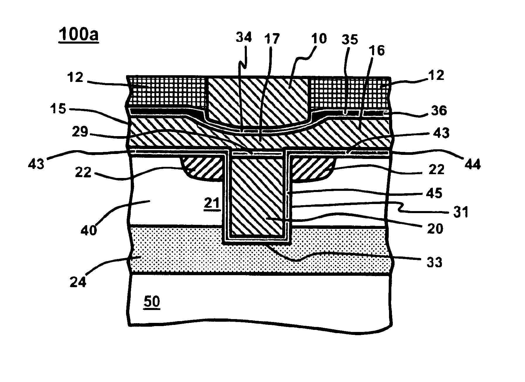
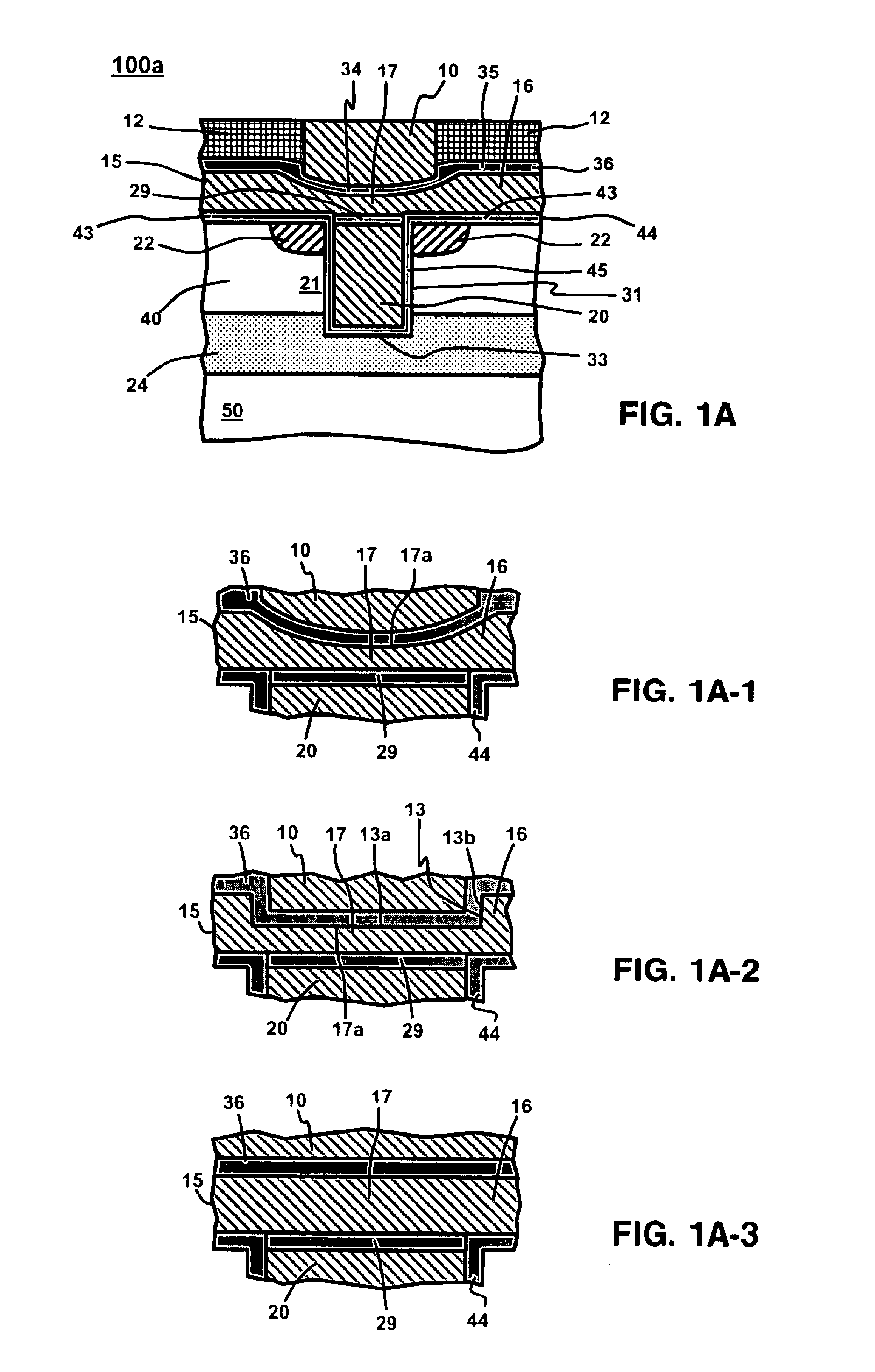
[0039]Referring to FIGS. 1A through 1D, there are shown cross sectional view of a single transistor non-volatile memory cell in accordance with this invention. Memory cell 100a in FIG. 1A comprises a bulk material 50, which can be either a semiconductor material, such as silicon, or an insulator, such as silicon oxide, silicon sulfide or other dielectrics well-known in the art. For the preferred embodiment, the bulk material 50 can be silicon of a first conductivity type (p-type hereinafter) with a lower doping level in the range between about 1E15 atom / cm−3 to about 5E17 atom / cm−3. On the bulk material 50 is a first semiconductor layer 40 of the first conductivity type with a higher doping level than the bulk material 50 and is in the range between about 5E15 atom / cm−3 to about 5E18 atom / cm−3. The thickness of the first layer 40 can be on the order of about 0.2 μm to about 4 μm. Both the bulk material 50 and the first semiconductor layer 40 are collectively referred to as substrate...

second embodiment

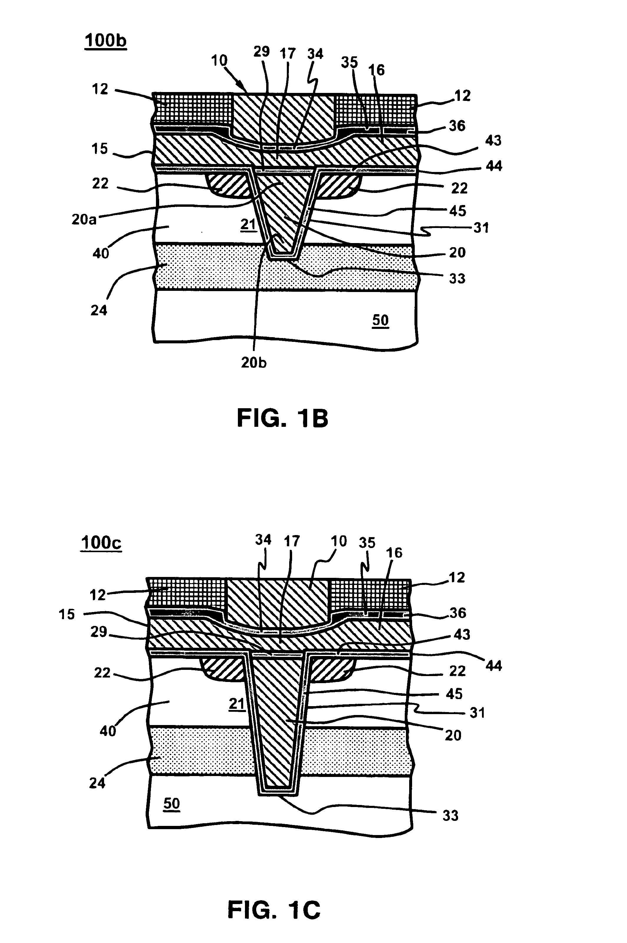
[0044]FIG. 1E presents cross sectional view of a single transistor non-volatile memory cell 100e in accordance with the present invention, wherein the memory cell 100e comprises similar provisions as defined in the memory cell 100a in FIG. 1A except with a major difference on the scheme dividing neighboring cells. The memory cell 100e define cell active region 4 through the provision of isolation regions 5 formed by well-known technique such as LOCOS process or shallow trench isolation process (“STI” hereinafter). In a preferred embodiment, the isolation region 5 is form in STI as it can be more precisely formed at smaller design rules. The STI is substantially in a rectangular shape with a thickness on the order of about 0.2 μm and a width of about 0.1 μm, and is typically made from insulator such as oxide or other dielectrics well-known in the art. The object in this embodiment is to minimize capacitive coupling between control gate 15 and memory well 40 in parasitic capacitive co...


PUM


Abstract

A method of forming an array of floating gate memory cells, and an array formed thereby, wherein each memory cell includes an electrical conductive floating gate formed in a trench in a semiconductor substrate, and an electrical conductive control gate having a portion disposed over and insulated from the floating gate. An electrical conductive tunneling gate is disposed over and insulated from the control gate by an insulating layer to form a tri-layer structure permitting both electron and hole charges tunneling through at similar tunneling rate. Spaced apart source and drain regions are formed with the source region disposed adjacent to and insulated from a lower portion of the floating gate, and with the drain region disposed adjacent to and insulated from an upper portion of the floating gate with a channel region formed therebetween and along a sidewall of the trench.

Description

TECHNICAL FIELD[0001]The present invention deals with nonvolatile memory, and relates more specifically to Electrically Programmable Read Only Memories (EPROM) and Electrically Erasable and Programmable Read Only Memories (EEPROM). More particularly, the present invention relates to memory cell architecture and methods forming cells and arrays of nonvolatile memory cell with floating gate.BACKGROUND OF THE INVENTION[0002]Non-volatile semiconductor memory cells using a floating gate to store charges thereon and memory arrays of such non-volatile memory cells formed in a semiconductor substrate are well known in the art. Typically, the memory cell is electrically programmable and erasable by transporting charges in and out of a floating gate that is electrically insulated from but capacitively coupled to the surrounding electrodes. The amounts of charges retained in the floating gate define the states of a memory cell. Typically, the states thus defined can be either two levels or mor...

Claims


Application Information

Patent Timeline
Patent Type & Authority Patents(United States)
IPC IPC(8): H01L29/66H01L29/40H01L21/70H01L29/423H01L27/115H01L21/8247H01L29/788
CPCH01L27/115H01L27/11521H01L29/42336H01L29/7885H10B69/00H10B41/30
Inventor WANG, CHIH-HSIN
Owner MARVELL ASIA PTE LTD
Why Eureka
Try Eureka