

Method and system to process semiconductor wafers
a technology of semiconductor wafers and processing methods, applied in the field of semiconductor manufacturing, can solve problems such as developing into more severe problems, and achieve the effects of preventing damage to the wafers, preventing the interruption of an already started process, and smooth and flexible recovery of the system
- Summary
- Abstract
- Description
- Claims
- Application Information
AI Technical Summary
Benefits of technology
Problems solved by technology
Method used
Image

Examples
Embodiment Construction
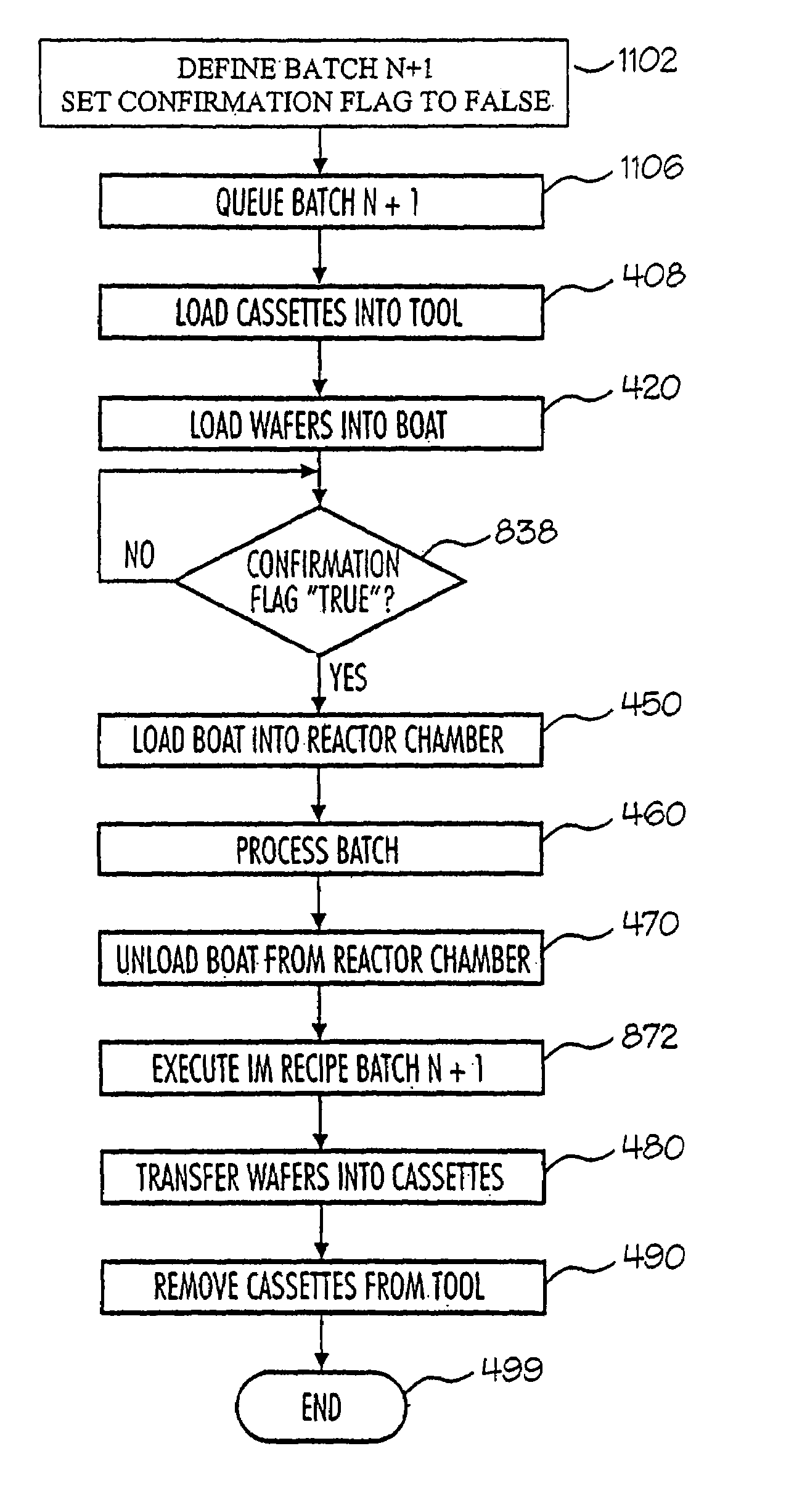
[0026]A method of the present invention includes a method to prohibit the loading and processing of wafers prior to the start of processing when an error in the process tool occurs. The method can be used in any one of a number of systems where work pieces are processed in a processing station. The method can be used for single wafer processing tools and for batch processing tools. Further, the method can advantageously be applied on tools comprising a plurality of processing stations. Interruption of the processing in such a multi-station tool requires an elaborate recovery procedure to bring the wafers of which the processing has been interrupted in a defined state and the present invention can be beneficially applied to such multi-station process tools. The examples presented in the following figures relate to batch furnaces and are for illustrative purposes only and are not intended to limit the application of the present invention to such examples.
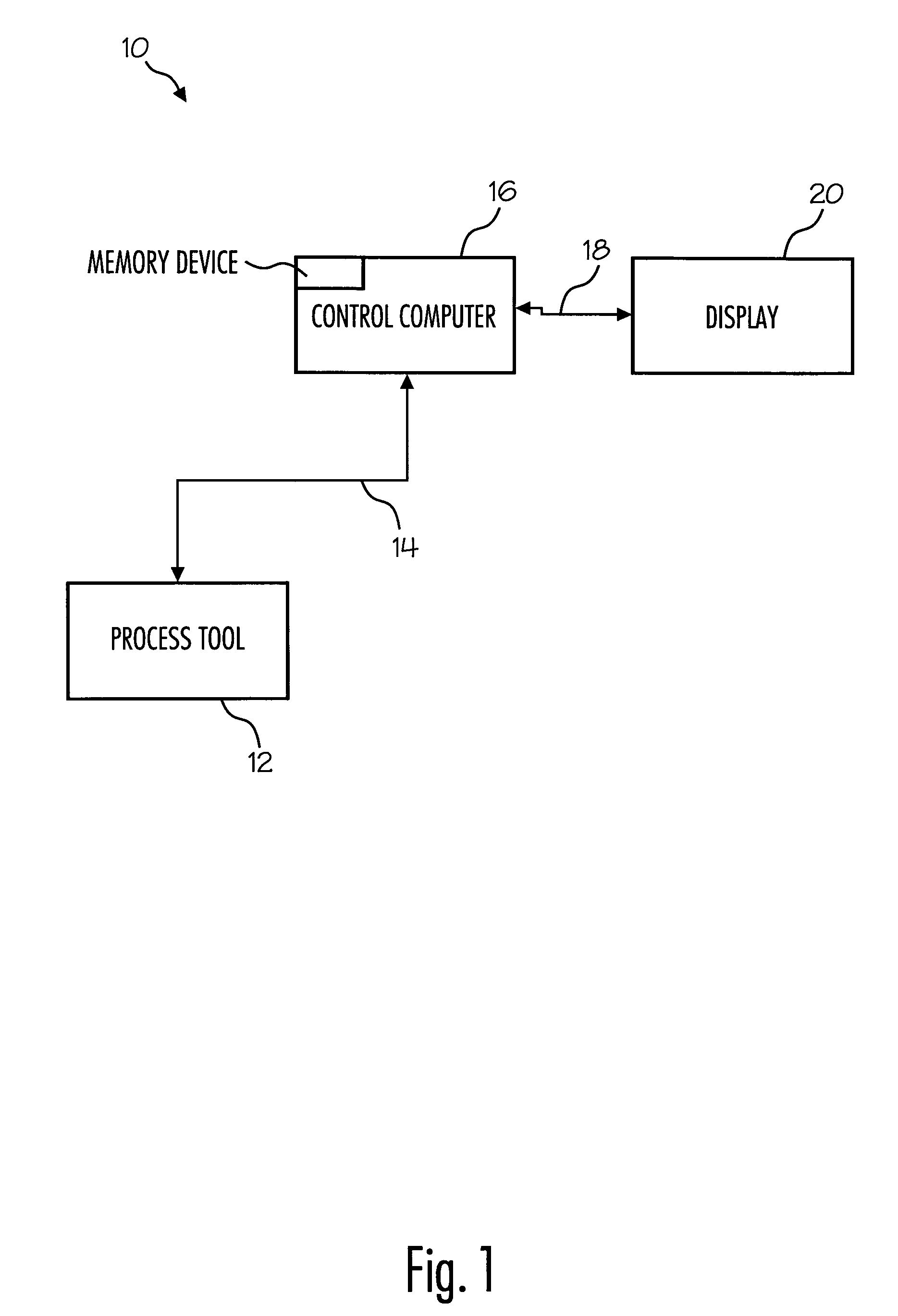
[0027]For example, FIG. 1 is a...
PUM
 Abstract
Description
Claims
Application Information