Optical detection device for detecting an intensity of a light beam and for detecting data transmitted by the light beam

a technology of optical detection and light beam, which is applied in the direction of optical radiation measurement, instruments, television systems, etc., can solve the problems of time-consuming and expensive, inaccurate, and inconvenient to take, and achieve the effect of reducing the error rate of data retrieved, accurate, and accurate adjustmen

Inactive Publication Date: 2006-03-07
DEUTSCHE THOMSON-BRANDT GMBH +1
View PDF7 Cites 26 Cited by
  • Summary
  • Abstract
  • Description
  • Claims
  • Application Information

AI Technical Summary

Benefits of technology

[0014]It is the object of the present invention to provide an optical detection means and a method for operating same, so that in addition to detecting data transmitted by the beam of light, a more effective form of aligning the light beam in an optimum manner is made possible with the optical detection means.
[0045]One of the considerations on which the present invention is based is that the provision of additional detection diodes in the detection window initially indeed results in additional expenditure and in a reduction of the area that may be effectively used for data detection, but that these disadvantages are by far outweighed by the fact that this array of additional detection diodes in the detection window enables more effective, or less expensive, control of the alignment of the light beam transmitting the data with the detection window. For example, in most cases it is not required, for controlling the alignment of the beam of light with the detection window, to detect the intensity of the light beam in the detection window at the same readout speed as the data rate, which is mostly high, at which the data is transmitted. This slower readout speed designed only for aligning the light beam with the detection window, however, enables that the detection diodes additionally inserted may have smaller surface areas since they can integrate, or sum up, the detected light over a longer period. Due to the slower readout of the array of additional detection diodes, the readout expenditure of these detection diodes is also smaller, and a multiplexed readout operation of this array is possible, whereby for reading out the additional array, e.g. only one additional output, or one additional pin, is required. Due to the fact that the additional diodes are arranged directly in the detection window provided for detecting the light beam transmitting the data, it is furthermore not required to produce additional light beams besides the light beam transmitting the data. Since the alignment of the beam of light with the detection window may be controlled by means of the spatial intensity distribution of the light beam transmitting the data in the detection window, the spatial intensity distribution being detected by the array of additional detection diodes, it is not required to subdivide the area of the detection window used for data detection into several parts, so that only a fast, and thus more expensive, readout circuit is required. In addition, the detection of the intensity of the light beam transmitting the data in the detection window itself by an array of additional detection diodes enables the detection of the center of intensity, which information may again be used in many applications for alternatively controlling the alignment of the light beam with the detection window.

Problems solved by technology

With all these applications for optical detectors there is a problem of fixedly mounting the optical detector in relation to the light beam to be detected so that the light beam is in optimum alignment with the optical detector.
This requires, e.g., time-consuming and expensive, since precise, adjustment in the assembly of the optical device wherein the optical detector is used, or requires time-consuming and costly precautions to be taken against thermal drifts or other application-specific operational incidents, such as precautions against misalignment of the light beam relative to the optical detector, or other factors negatively influencing the readout.
In addition, optical offsets due to optical variations in the substrate thickness on the storage medium and tilts of the optical plate from a target position have a negative impact on the error rate of the data retrieved, since these events cannot be detected.
The result is a time-consuming and costly manufacturing process eliminating these sources of error by means of precise adjustment, expensive components and more costly tracking and focus control.
Additional problems result from the constantly increasing requirements placed upon the storage density and compactness of the optical storage plate.
Previous detectors have offered no possibility of detecting this.
Again, this results in increased error rates, since, for example, a pit which may be present on the adjacent track may lead to a false readout result if no pit is present on the track to be read out, and at the same time this restricts the track pitch on the data carrier, which, in turn, plays a decisive role in determining the storage capacity of the medium.
In addition, a disadvantage of the previous diode structures is the high expenditure required to obtain information from the light beam received about a misalignment, and / or correction signals for the latter.

Method used


Image

  • Optical detection device for detecting an intensity of a light beam and for detecting data transmitted by the light beam
  • Optical detection device for detecting an intensity of a light beam and for detecting data transmitted by the light beam
  • Optical detection device for detecting an intensity of a light beam and for detecting data transmitted by the light beam

Examples


Embodiment Construction

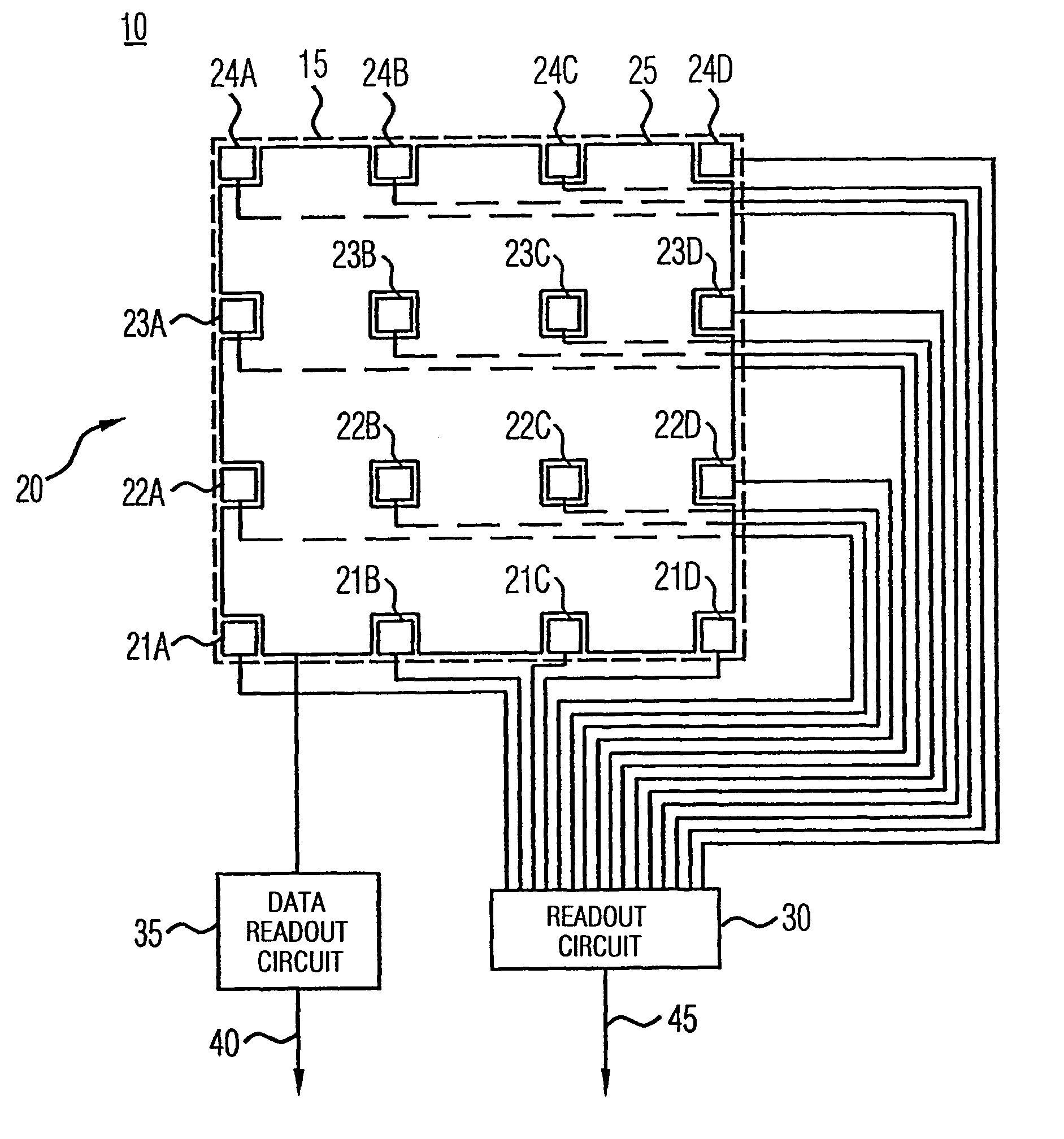
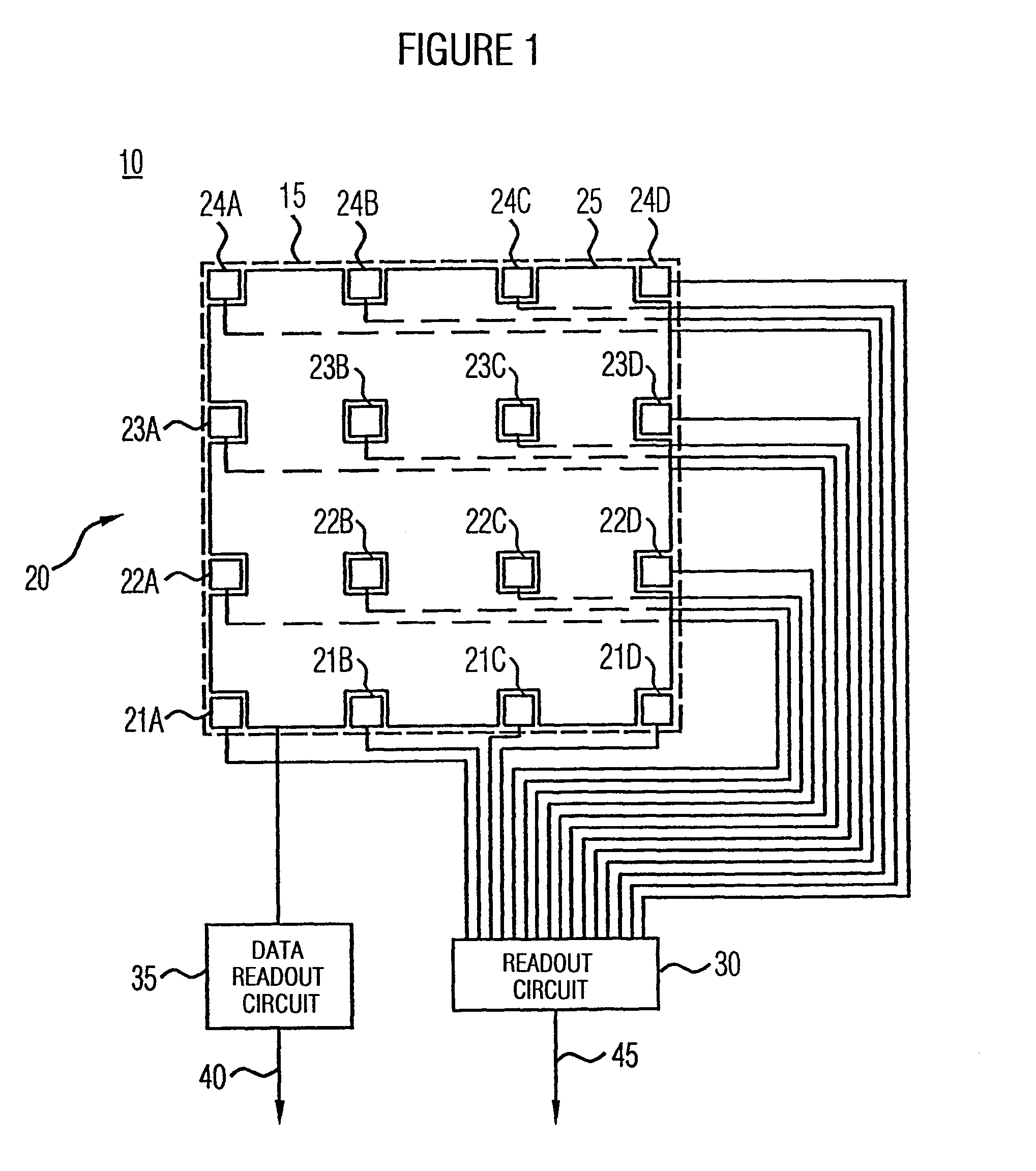
[0065]FIG. 1 initially shows an optical detection device in accordance with an embodiment of the present invention, generally indicated by 10. In a detection window 15 provided for detecting a light beam transmitting data, the optical detection device 10 includes a 4×4 array 20 of detection diodes 21a, 21b, 21c, 21d, 22a, 22b, 22c, 22d, 23a, 23b, 23c, 23d, 24a, 24b, 24c, 24d, the second figure, respectively, indicating a line number, and the letter indicating a column number. In addition, the optical detection device 10 includes a detection diode 25 occupying, or covering, in terms of surface area, that part of the detection window 15 which is not occupied by the diode array 20. The detection diodes 21a–24d are connected to a readout circuit 30, whereas the detection diode 25 is connected to a data readout circuit 35. The readout speeds of the readout circuits 30 and 35 differ. The data readout circuit 35 has a readout speed which is sufficiently high to be able to scan the data, wh...


PUM


Abstract

An optical detection device for detecting an intensity of a light beam in a detection window and for detecting data transmitted by the light beam includes a first detection diode and an array of at least two second detection diodes in a detection window. In addition, provision is made for a first readout circuit connectable to the first detection diode, for reading out the first detection diode at a first readout speed to detect the data, and for a second readout circuit connectable to the second detection diodes, for reading out the second detection diodes at a second readout speed smaller than the first readout speed, so as to detect the intensity of the light beam. A fundamental consideration underlying the present invention is that although the provision of additional detection diodes in the detection window initially is associated with additional expense and a reduction of the surface area of the detection window which may effectively be utilized for data detection, these disadvantages are outweighed however, by the fact that this array of additional detection diodes in the detection window enables more effective and / or less expensive control of the alignment of the light beam transmitting the data with the detection window.

Description

CROSS-REFERENCE TO RELATED APPLICATION[0001]This application is a continuation of copending International Application No. PCT / EP03 / 05379, filed May 22, 2003, which designated the United States, Japan, China and The Republic of Korea and was not published in English and is incorporated herein by reference in its entirety.BACKGROUND OF THE INVENTION[0002]1. Field of the Invention[0003]The present invention relates to optical detection means, such as optical scanner or pick-up systems in CD (compact disc) and DVD (digital versatile disc) equipment or optical receivers in optical transmission lines.[0004]2. Description of Prior Art[0005]Driven by the increasing multi-media demands with regard to photo, audio and video, the memory requirement is currently growing at an exponential rate. Optical memory systems here constitute a particularly attractive solution between magnetic tape storage media and hard discs. With access times in the range of milliseconds, which are only slightly higher...

Claims


Application Information

Patent Timeline
Patent Type & Authority Patents(United States)
IPC IPC(8): G01J1/42G11B7/125G11B7/13
CPCG11B7/131G11B7/126G01J1/02H01L31/10
Inventor HEHEMANN, INGOBROCKHERDE, WERNERKEMNA, ARMINHOFMANN, HOLGERRICHTER, HARTMUT
Owner DEUTSCHE THOMSON-BRANDT GMBH
Why Eureka
Try Eureka