Electro-optical device and method for manufacturing the same

a technology of optical devices and optics, applied in the field of electric devices, can solve the problems of large area required in the connection portion, inability to apply to a high-resolution display, and wire connection problems

Inactive Publication Date: 2006-07-25
SEMICON ENERGY LAB CO LTD
View PDF251 Cites 15 Cited by
  • Summary
  • Abstract
  • Description
  • Claims
  • Application Information

AI Technical Summary

Benefits of technology

[0009]The present invention is to perform miniaturization, light weighting and thinning of a display, by arranging semiconductor chips as provided in the above main board in at least one substrate in the a liquid crystal display which a liquid crystal material is held between a pair of substrates. In particular, these chip are provided in a substrate (board) in which an active matrix circuit is formed. Also, a driving circuit for driving the active matrix circuit is formed by using thin film transistors (TFTs).

Problems solved by technology

Also, since a width of wirings (interconnection) extending from the active matrix circuit get small to improve an opening (aperture) rate and the total number of wirings exceeds 1000, there is a technical problem in wiring connection.
Further, a large area is required in a connection portion.
Therefore, it cannot be applied to a high resolution display which has a pixel pitch of 60 μm or shorter and miniaturization of a display cannot be performed, so that a TFT using an amorphous silicon which can be formed at a low temperature is used in such display.
Since an external type semiconductor chip as described above is not used in such display device, a display gets relatively small.
In the second type display, however, further miniaturization, light weighting and thinning are not performed insufficiently.

Method used


Image

  • Electro-optical device and method for manufacturing the same
  • Electro-optical device and method for manufacturing the same
  • Electro-optical device and method for manufacturing the same

Examples


embodiment 1

[Embodiment 1]

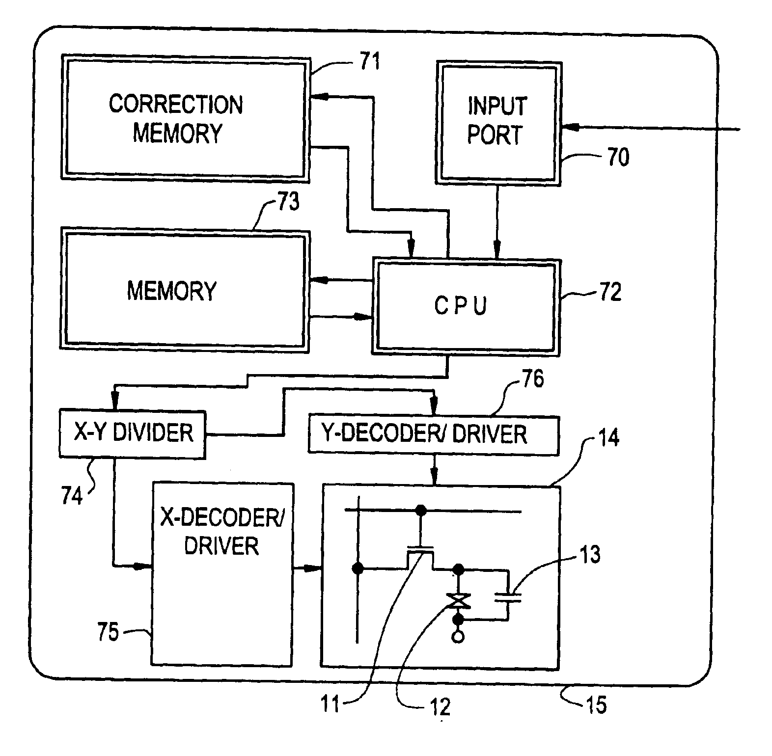
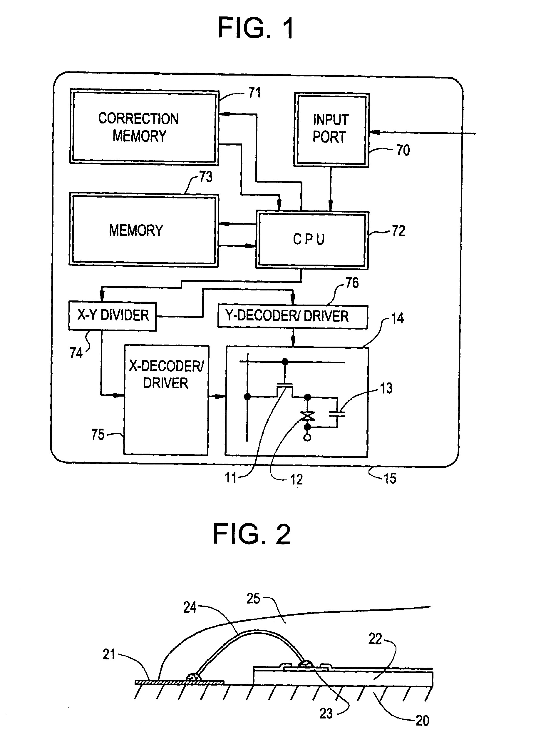
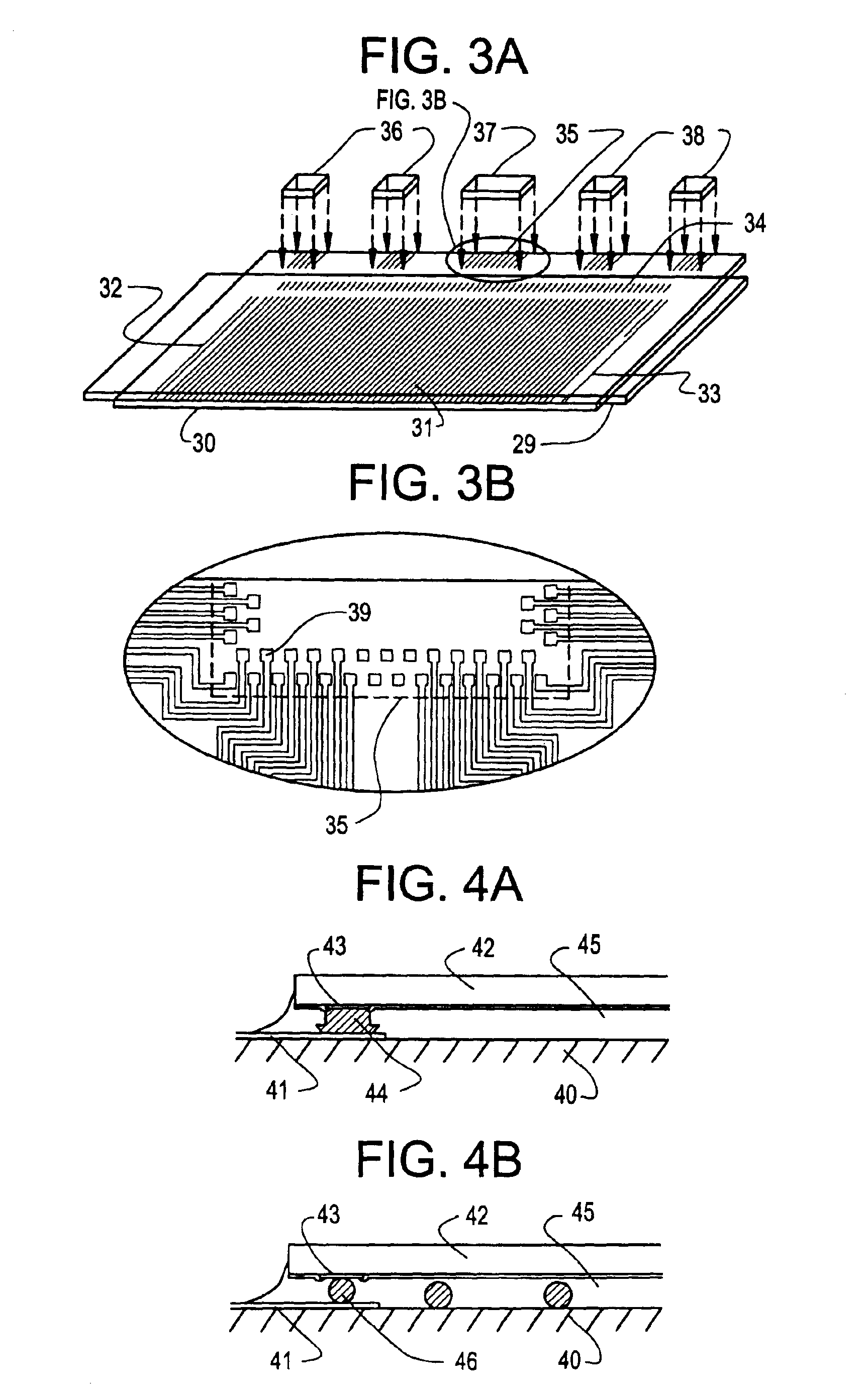
[0026]FIG. 3 shows a schematic view of a liquid crystal display panel according to an embodiment of the present invention. In FIG. 3, a substrate (board) 29 is placed opposite to the substrate (board) 30 and a liquid crystal material is held between the substrates 29 and 30. An active matrix circuit 31 and peripheral driving circuits 32 to 34 for driving the active matrix circuit 31 are formed using thin film transistors (TFTs) on the substrate 30 such as a glass substrate. Also, main memory chips 36, MPU (microprocessing unit) 37 or CPU (central processing unit) and correction memories 38 are adhered to a surface of the substrate 30 in which the above circuits 31 to 34 are formed, and electrically connected with the above circuits 31 to 34. For example, when chips are connected with a substrate by a FCOG, a wiring terminal portion (wiring connection pad) 39 (corresponding to a wiring portion 41 of FIGS. 4A and 4B) made of the ITO are formed in a portion 35 of the subs...

embodiment 2

[Embodiment 2]

[0030]A panel as shown in FIG. 3 is manufactured. The active matrix circuit 31 and the peripheral driving circuits 32 to 34 are formed using TFTs on the substrate 30. The main memory chips 36, the MPU (microprocessing unit) 37 or CPU (central processing unit) and the correction memories 38 are adhered to a surface of the substrate 30 in which the above circuits 31 to 34 are formed, and electrically connected with the wiring terminal portion (wiring connection pad) 39 (corresponding to the terminal electrode 21) which is made of an aluminum alloy thin film and formed on the substrate 40 by a wire bonding as shown in FIG. 2. A gold fine line is used as a bonding wire.

embodiment 3

[Embodiment 3]

[0031]In this embodiment, chips are adhered to a TFT circuit (monolithic type active matrix circuit) substrate by a FCOG, to construct further improved circuit. A process for manufacturing a monolithic type active matrix circuit will be described later using FIGS. 5A to 5G. A silicon oxide film having a thickness of 1000 to 3000 Å is formed as a base oxide film 502 on a substrate (Corning 7059) 501. A method for forming this oxide film may include a sputtering in an atmosphere containing oxygen or a plasma CVD (Chemical Vapor Deposition).

[0032]A silicon film having amorphous or crystalline is formed at a thickness of 300 to 1500 Å, preferably 500 to 1000 Å by a plasma CVD or a low pressure CVD (LPCVD). In order to form an crystalline silicon film, after forming an amorphous silicon film, a laser or an intense light equivalent to the laser may be irradiated (light annealing), or thermal annealing may be performed at 500° C. or higher for a long time of period. Also, aft...


PUM

PropertyMeasurementUnit
thicknessaaaaaaaaaa
wavelengthaaaaaaaaaa
sheet resistanceaaaaaaaaaa

Abstract

Using thin film transistors (TFTs), an active matrix circuit, a driver circuit for driving the active matrix circuit or the like are formed on one substrate. Circuits such as a central processing unit (CPU) and a memory, necessary to drive an electric device, are formed using single crystalline semiconductor integrated circuit chips. After the semiconductor integrated circuit chips are adhered to the substrate, the chips are connected with wirings formed on the substrate by a chip on glass (COG) method, a wire bonding method or the like, to manufacture the electric device having a liquid crystal display (LCD) on one substrate.

Description

[0001]This application is a Continuation of Ser. No. 08 / 350,168, filed Nov. 30, 1994, now abandoned.BACKGROUND OF THE INVENTION[0002]1. Field of the Invention[0003]The present invention relates to an electric device having a non-light emitting type display such as a liquid crystal display, which an active matrix circuit is formed on a substrate by using thin film transistors (TFTs). In particular, the active matrix circuit of the electric device according to the present invention is drive-controlled by a driving circuit constructed by TFTs formed on the same substrate.[0004]2. Description of the Related Art[0005]Recently, a liquid crystal display is used as a display in an various electric devices of a portable type (for example, a personal computer, a word processor, or an electric pocket note book), by utilizing that the liquid crystal display is thin and light in weight. In particular, since an active matrix type liquid crystal display which controls each pixel one by one using T...

Claims


Application Information

Patent Timeline
Patent Type & Authority Patents(United States)
IPC IPC(8): G02F1/1345G02F1/1343H01L21/77H01L21/84H01L27/13H01L29/423H01L29/49
CPCH01L29/42384H01L29/4908H01L27/1255H01L2224/48091H01L2224/73204H01L2224/48464H01L2924/00014H01L27/1251
Inventor YAMAZAKI, SHUNPEITAKEMURA, YASUHIKO
Owner SEMICON ENERGY LAB CO LTD
Why Eureka
Try Eureka