Supercharge Your Innovation With Domain-Expert AI Agents!

Semiconductor storage device

a technology of semiconductors and storage devices, applied in the field of semiconductor storage devices, can solve the problems that conventional fbc devices had no means to know the characteristics of memory cells themselves

Inactive Publication Date: 2006-08-22
KK TOSHIBA
View PDF8 Cites 6 Cited by
  • Summary
  • Abstract
  • Description
  • Claims
  • Application Information

AI Technical Summary

Problems solved by technology

Therefore, conventional FBC devices had no means to know the characteristics of memory cells themselves.

Method used


Image

  • Semiconductor storage device
  • Semiconductor storage device
  • Semiconductor storage device

Examples


first embodiment

(First Embodiment)

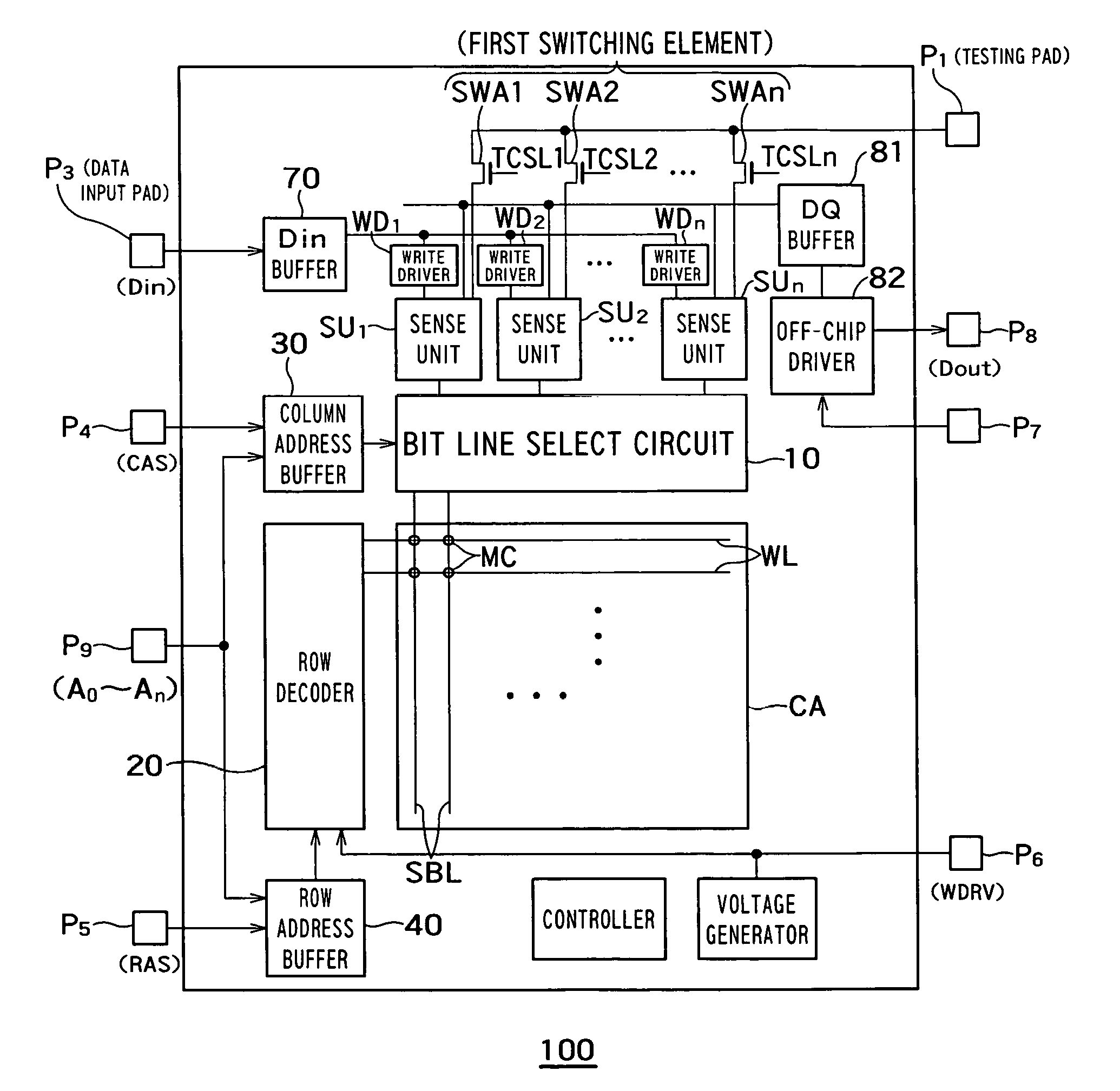
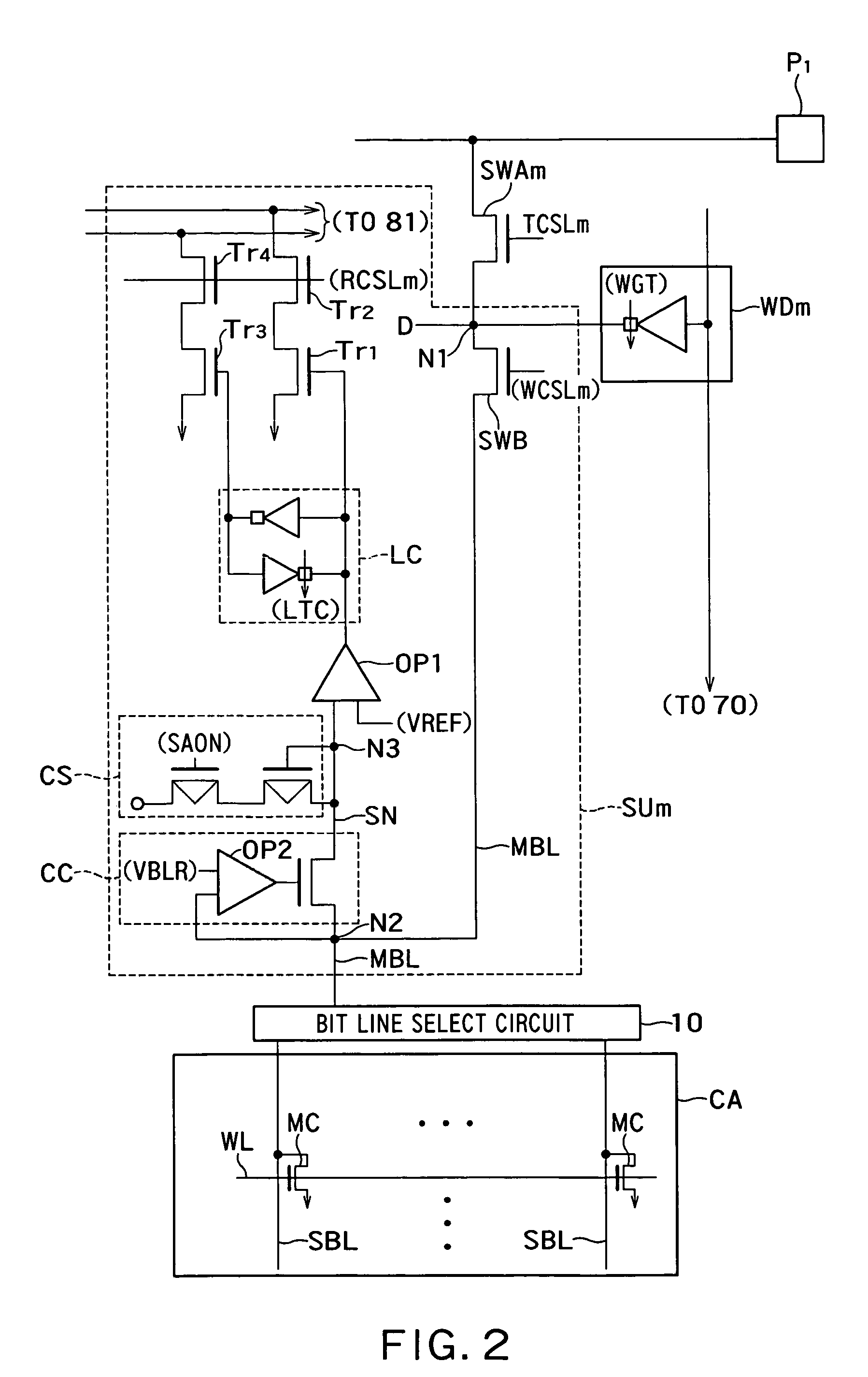
[0026]FIG. 1 is a block diagram of a semiconductor storage device 100 according to the first embodiment of the invention. The semiconductor storage device 100 comprises memory cells MC, a memory cell array CA, word lines WL, sub-bit lines SBL, a bit line select circuit 10, a row decoder 20, a column address buffer 30, a row address buffer 40, sense units SU1˜SUn, write drivers WD1˜WDn, a Din buffer 70, a DQ buffer 81, an off-chip driver 82, pads P1˜P8, and switching elements SWA1˜SWAn.

[0027]The semiconductor storage device 100 can be, for example, a FBC memory device or a DRAM. Memory cells store data by accumulating or releasing electric charges. The memory cells may be, for example, FBC memory cells or DRAM cells. The memory cell array CA includes a plurality of memory cells MC in a matrix arrangement. Each word line WL is connected to memory cells MC on individual rows of the memory cell array CA. Each sub-bit line SBL is connected to memory cells MC on individu...

second embodiment

(Second Embodiment)

[0068]FIG. 5 is a circuit diagram showing a semiconductor storage device 200 according to the second embodiment of the invention. The second embodiment is different from the first embodiment in including witching elements SWC and SWD. The other components of the second embodiment may be identical to the components of the first embodiment.

[0069]The switching element SWC as the second switching element is interposed in the main bit line MBL from the write drive WDm to the bit line select circuit 10. The switching element SWC can switch between the switching element SWB and the node N2.

[0070]The switching element SWD as the third switching element has one end connected between the clamp circuit CC and the operational amplifier OP1 and the other end connected to the main bit line MBL from the driver WDm to the switching element SWC. The switching elements SWC and SWD may be MOSFETs, for example.

[0071]Operations of the second embodiment will be explained below.

[0072](N...

third embodiment

(Third Embodiment)

[0084]FIG. 6 is a block diagram of a semiconductor storage device 300 according to the third embodiment of the invention. The third embodiment is different from the first embodiment in commonly using the data input pad P3 as the test pad as well. The other components of the third embodiment are identical to those of the first embodiment.

[0085]FIG. 7 is a diagram showing the relationship among the sense units Sum, the write driver WDm and the switching element SWAm in greater detail.

[0086]In the third embodiment, one end of the switching element SWAm is connected to the output of the write driver WDm, and the other end thereof is connected to the data input pad P3. That is, the switching element SWAm is connected between the data input pad P3 and the node N1 to bypass the Din buffer 70 and the write driver WDm.

[0087]In the test write mode and the test read mode of the third embodiment, a voltage is applied externally through the data input pad P3, and the cell curre...


PUM


Abstract

A semiconductor storage device comprises memory cells that store data by accumulating or releasing an electric charge; a memory cell array having a matrix arrangement of the memory cells; a plurality of word lines connected to memory cells aligned on rows of the memory cell array; a plurality of sub-bit lines connected to memory cells aligned on columns of the memory cell array; a bit line select circuit selecting the sub-bit line of a column; a main bit line connected to the sub-bit line selected by the bit line select circuit; a sense line detecting the potential of the sub-bit line selected by the bit line select circuit via the main bit line and reading data out of the memory cell; a write driver applying a voltage to the sub-bit line selected by the bit line select circuit via the main bit line and writing data into the memory cell; and a first switching element connected to the main bit line and turning on when the current flowing in the memory cell is detected externally via the sub-bit line without the use of the sense line or when a voltage is applied to the memory cell externally via the sub-bit line without the use of the write driver.

Description

CROSS-REFERENCE TO RELATED APPLICATION[0001]This application is based upon and claims the benefit of priority from the prior Japanese Patent Applications No. 2004-219783, filed on Jul. 28, 2004, the entire contents of which are incorporated herein by reference.BACKGROUND OF THE INVENTION[0002]1. Field of the Invention[0003]The present invention relates to a semiconductor storage device.[0004]2. Background Art[0005]FBC (Floating Body Cell) has recently been developed as a densely integrative memory cell in the place of DRAM. FBC memory devices are composed of transistors formed on SOI substrates. FBC memory devices store data “1” or data “0” by accumulating or releasing holes in or from their floating bodies.[0006]Upon testing a conventional FBC memory device, data was written in a memory cell by a write driver prepared for normal operation, and data was read out from the memory cell by a sense amplifier prepared for normal operation.[0007]Therefore, conventional FBC devices had no m...

Claims


Application Information

Patent Timeline
Patent Type & Authority Patents(United States)
IPC IPC(8): G11C11/34
CPCG11C11/404G11C29/50G11C11/4094G11C2211/4016
Inventor HIGASHI, TOMOKIOHSAWA, TAKASHI
Owner KK TOSHIBA
Features
  • R&D
  • Intellectual Property
  • Life Sciences
  • Materials
  • Tech Scout
  • Unparalleled Data Quality
  • Higher Quality Content
  • 60% Fewer Hallucinations
Learn More