EMI absorbing shielding for a printed circuit board

a printed circuit board and shielding technology, applied in the field ofemi shielding, can solve the problems of increasing the cost of manufacturing electronic equipment, increasing the cost of electronic equipment such as cell phones, personal digital assistants, and high cost of electronic equipment, and achieves high permittivity and permeability, high resistivity, and the effect of dispersing electromagnetic energy into hea

Inactive Publication Date: 2006-10-31
WAVEZERO +1
View PDF6 Cites 71 Cited by
  • Summary
  • Abstract
  • Description
  • Claims
  • Application Information

AI Technical Summary

Problems solved by technology

In virtually all cases, the existing solutions are expensive and add to the cost of manufacturing electronic equipment such as cell phones, personal digital assistants, laptop computers, set-top boxes, cable modems, networking equipment including switches, bridges, and cross-connects.
The material was shown to be expensive, difficult to use, and subject to inferior performance due to cracking of the metallized layer.
The resultant assembly of the EMI shielding and the electronic component provides adequate shielding for many applications; however, as the frequency of chips increase and the data transmission rates increase, the creation of errant radiation (EMI) becomes much easier and more harmful to circuits and components located nearby.
Thus, in general, conventional EMI solutions will increasingly find themselves inadequate for purposes of immunity and indeed, radiated emissions may also become an increasing issue.
Furthermore, for microwave devices, especially those that operate of have harmonic frequencies above about 10 GHz. radiated emissions will be a significant concern.
In general, there is nothing to contain the radiation escaping from the bottom of the chip except for the phenomena of reflection from the ground plane (the “image” plane) which can, in some situation, improve the radiation emissions problem but is problematical from a design and manufacturing point to achieve.
In general, only sophisticated numerical analysis codes can predict these resonances.
More importantly, there are not any readily acceptable methods to altering the frequency of the resonances or their amplitudes.
The presence of these difficult-to-treat resonances makes EMC design difficult.

Method used


Image

  • EMI absorbing shielding for a printed circuit board
  • EMI absorbing shielding for a printed circuit board
  • EMI absorbing shielding for a printed circuit board

Examples


Embodiment Construction

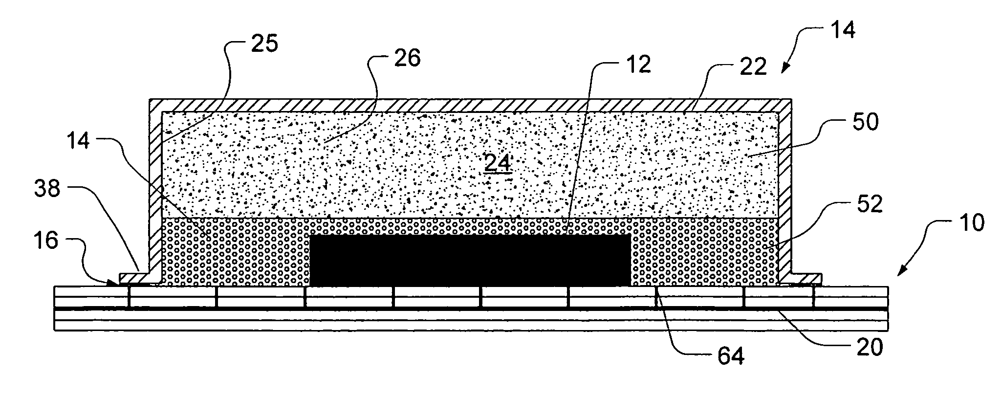
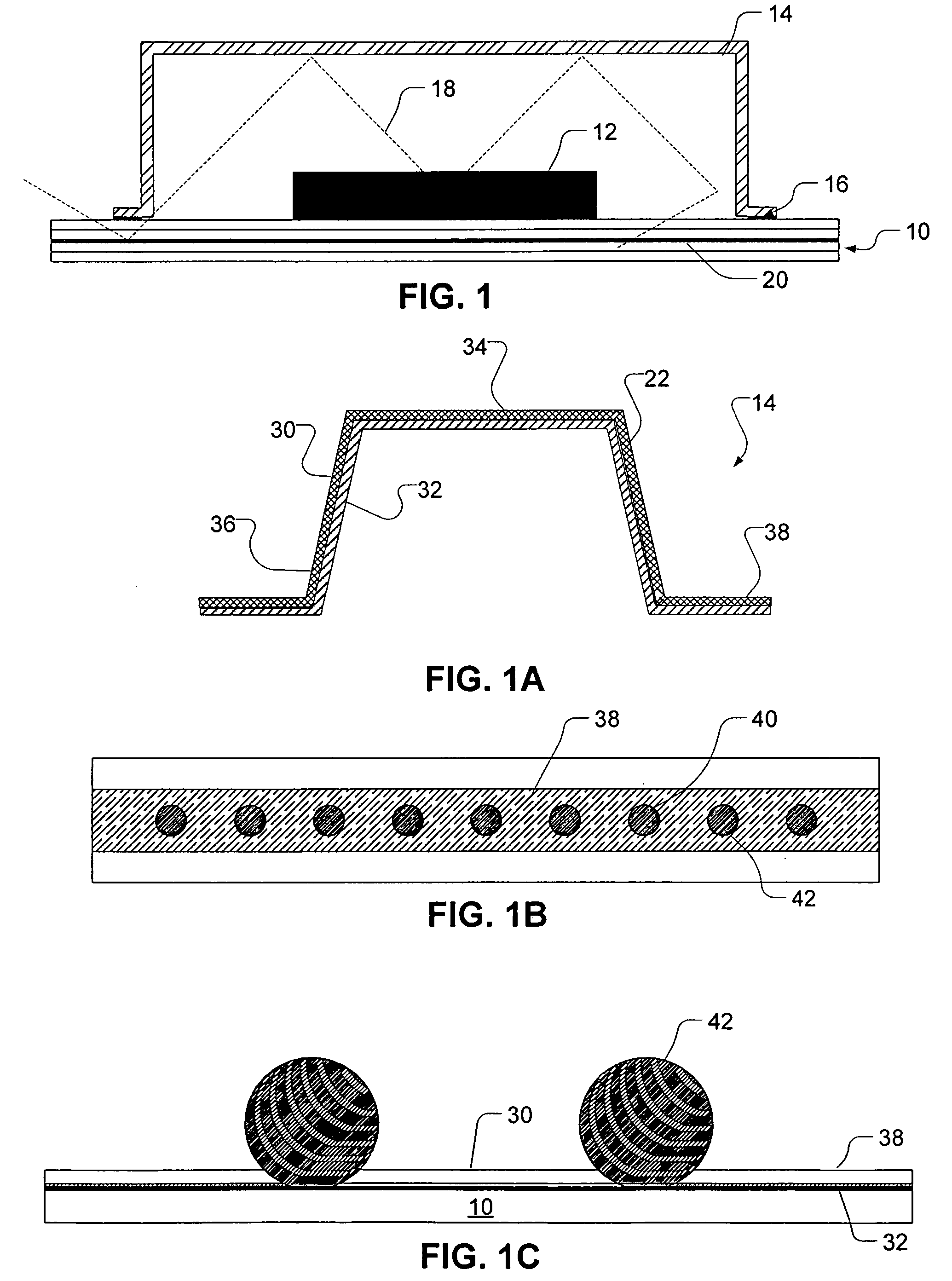
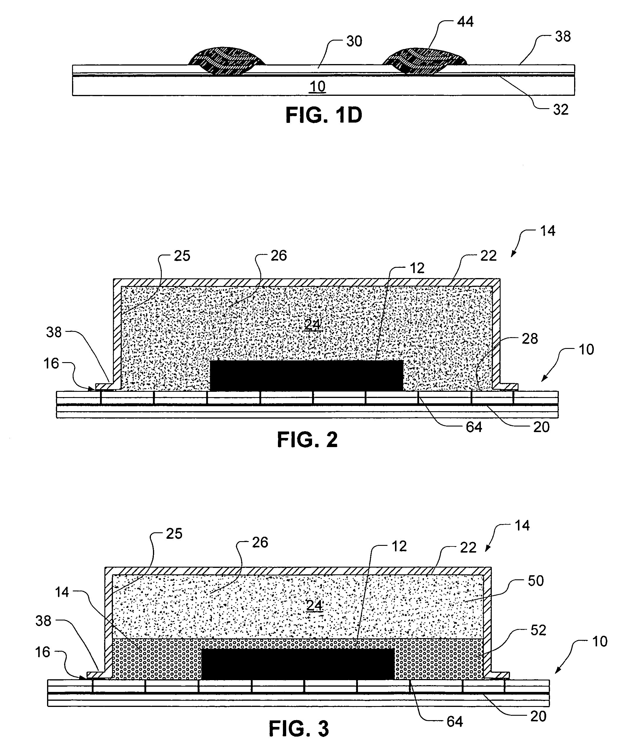
[0043]The present invention provides printed circuit boards and EMI shields that comprise an integration of a shield body (e.g., a shaped resin or polymer substrate such as a metallized thermoform) with an EMI absorbing material to provide an EMI shield that is effective in terms of both reflection and absorption of electric and magnetic fields emitted from an electronic component to mitigate the effects of chamber resonances.

[0044]The EMI shields of the present invention may comprise an EMI absorbing material. The EMI absorbing material may completely fill a space defined by the shield body, cover all inner and / or outer surfaces of the shield body, or cover only selected portions of the inner and / or outer surfaces of the shield body. Further, the EMI absorbing material may be locally placed for particular applications and still provide important EMI absorption.

[0045]EMI absorbing material typically have a high permittivity and permeability (i.e., good ability to store electric and ...


PUM


Abstract

The present invention provides printed circuit boards, EMI shields, and methods that provide an EMI absorbing material and an EMI reflecting material. In one embodiment, the EMI shield comprises a shield body and an EMI absorbing material coupled to the shield body.

Description

CROSS-REFERENCES TO RELATED APPLICATIONS[0001]The present application claims benefit to U.S. Provisional Patent Application Ser. No. 60 / 479,460, entitled “E-field and H-field EMI shielding for the printed circuit board,” filed Jun. 19, 2003, the complete disclosure of which is incorporated herein by reference.BACKGROUND OF THE INVENTION[0002]The present invention relates generally to EMI shielding. More specifically, the present invention relates to EMI shielding that comprises an absorbing material that is capable of absorbing electromagnetic radiation.[0003]All electronic products emit electromagnetic radiation, generally in the range of 50 MHz. to 1 GHz., but not limited to this range especially in light of the many advances in high-speed microprocessor design and the rapidly increasing capabilities of high-speed networking and switching. The problem of emittance of electromagnetic radiation is not new to designers of electronic equipment; indeed, significant efforts are taken to...

Claims


Application Information

Patent Timeline
Patent Type & Authority Patents(United States)
IPC IPC(8): H05K9/00H01P5/00H01P5/12H03H7/00H05KH05K5/02
CPCH05K9/0024H05K9/003H01L23/24H01L23/295H01L23/3135H01L23/315H01L23/552H01L2924/16251H01L2924/166H05K9/0031
Inventor ARNOLD, ROCKY R.
Owner WAVEZERO
Why Eureka
Try Eureka