

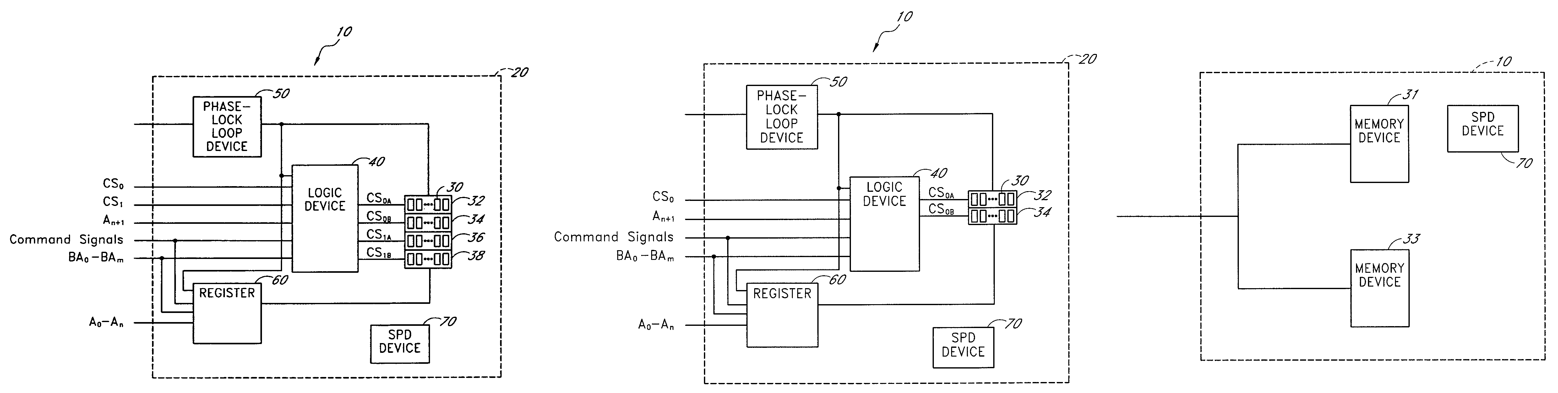
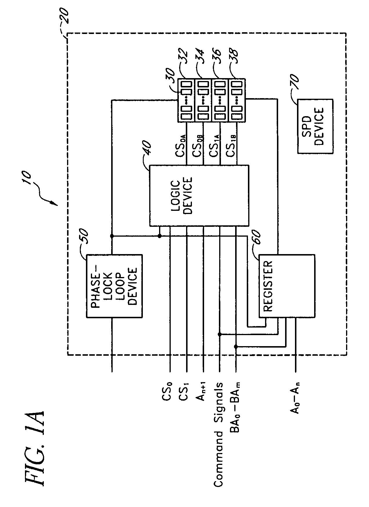
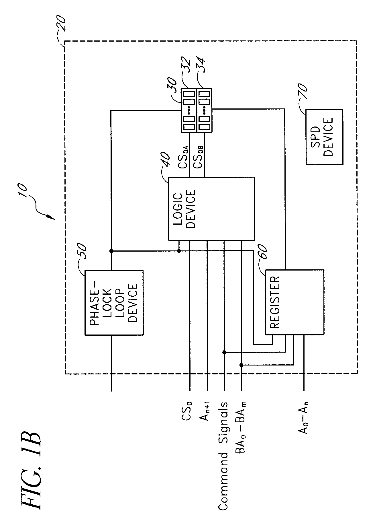
Memory module decoder
a memory module and decoder technology, applied in the field of memory module decoders, can solve the problem of limited memory density that can be incorporated in each memory slo
- Summary
- Abstract
- Description
- Claims
- Application Information
AI Technical Summary
Benefits of technology
Problems solved by technology
Method used
Image

Examples
example 1
[0100]
always @(posedge clk_in) begin rs0N_R rasN_R casN_R weN_R end / / Gated Chip Selectsassignpcs0a_1 = (~rs0_in_N & ~ras_in_N & ~cas_in_N) / / ref,md reg set| (~rs0_in_N & ras_in_N & cas_in_N) / / ref exit, pwr dn| (~rs0_in_N & ~ras_in_N & cas_in_N & ~we_in_N & a10_in) / / pchg all| (~rs0_in_N & ~ras_in_N & cas_in_N & ~we_in_N & ~a10_in & ~ba2_in) / / pchg single bnk| (~rs0_in_N & ~ras_in_N & cas_in_N & we_in_N & ~ba2_in) / / activate| (~rs0_in_N & ras_in_N & ~cas_in_N & ~ba2_in) / / xfr;assignpcs0b_1 = (~rs0_in_N & ~ras_in_N & ~cas_in_N) / / ref,md reg set| (~rs0_in_N & ras_in_N & cas_in_N) / / ref exit, pwr dn| (~rs0_in_N & ~ras_in_N & cas_in_N & ~we_in_N & a10_in) / / pchg all| (~rs0_in_N & ~ras_in_N & cas_in_N & ~we_in_N & ~a10_in & ba2_in) / / pchg single bnk| (~rs0_in_N & ~ras_in_N & cas_in_N & we_in_N & ba2_in) / / activate| (~rs0_in_N & ras_in_N & ~cas_in_N & ba2_in) / / xfr; / / ------------------------------------- always @(posedge_clk_in) begin a4_r a5_r a6_r a10_r ba0_r ...
example 2
[0102]
/ / latched a13 flags cs0, banks 0-3 always @(posedge clk_in) if (actv_cmd_R & ~rs0N_R & ~bnk1_R & ~bnk0_R) / / activate begin l_a13_00 end always @(posedge clk_in) if (actv_cmd_R & ~rs0N_R & ~bnk1_R & bnk0_R) / / activate begin l_a13_01 end always @(posedge clk_in) if (actv_cmd_R & ~rs0N_R & bnk1_R & ~bnk0_R) / / activate begin l_a13_10 end always @(posedge clk_in) if (actv_cmd_R & ~rs0N_R & bnk1_R & bnk0_R) / / activate begin l_a13_11 end / / gated casassign cas_i = ~(casN_R);assign cas0_o = ( ~rasN_R & cas_i) | ( rasN_R & ~l_a13_00 & ~bnk1_R & ~bnk0_R & cas_i) | ( rasN_R & ~l_a13_01 & ~bnk1_R & bnk0_R & cas_i) | ( rasN_R & ~l_a13_10& bnk1_R & ~bnk0_R & cas_i) | ( rasN_R & ~l_a13_11 & bnk1_R & bnk0_R & cas_i) ;assign cas1_o = ( ~rasN_R & cas_i) | ( rasN_R & l_a13_00 & ~bnk1_R & ~bnk0_R & cas_i) | ( rasN_R & l_a13_01 & ~bnk1_R & bnk0_R & cas_i) | ( rasN_R & l_a13_10 & bnk1_R & ~bnk0_R & cas_i) | (rasN_R & l_a13_11 & bnk1_R & bnk0_R...
PUM
 Abstract
Description
Claims
Application Information