Solid-state image-sensing device that compensates for brightness at edges of a display area and a driving method thereof

a solid-state image and display area technology, applied in the direction of television systems, instruments, gearing, etc., can solve the problem of increasing quantum noise, and achieve the effect of reducing sensitivity, low signal-to-noise ratio (snr), and not increasing quantum nois

Active Publication Date: 2007-03-20
SAMSUNG ELECTRONICS CO LTD
View PDF7 Cites 579 Cited by
  • Summary
  • Abstract
  • Description
  • Claims
  • Application Information

AI Technical Summary

Benefits of technology

[0009]The present invention provides a complementary metal-oxide semiconductor (CMOS) image sensor (CIS)-type solid-state image-sensing device that outputs image signals from the center and edges of an active pixel sensor (APS) array at a uniform level without a low signal-to-noise ratio (SNR) or decreased sensitivity at the edges of the APS array while producing a uniformly bright image on a screen without increasing quantum noise. The present invention also provides a method of driving a CIS-type solid-state image-sensing device that can output image signals from the center and edges of an APS array at a uniform level such that a uniformly bright image is displayed on a screen.
[0011]The APS array is divided into a plurality of groups, each including a plurality of rows, and the transmission control signals set non-uniform integration times for photodiodes of each of the groups and each of the rows of one of the groups, and set the same integration times for photodiodes disposed in the same column within each of the groups. The transmission control signal can set the integration times of side photodiodes of each of the rows of the groups to be longer than the integration times of photodiodes closer to the center of the APS array. Also, the transmission control signal can symmetrically set integration times of photodiodes disposed symmetrically about a central row of pixels of the APS array.

Problems solved by technology

However, even when employing these techniques, quantum noise increases during signal processing, thus leading to other problems such as a blinking screen.

Method used


Image

  • Solid-state image-sensing device that compensates for brightness at edges of a display area and a driving method thereof
  • Solid-state image-sensing device that compensates for brightness at edges of a display area and a driving method thereof
  • Solid-state image-sensing device that compensates for brightness at edges of a display area and a driving method thereof

Examples


Embodiment Construction

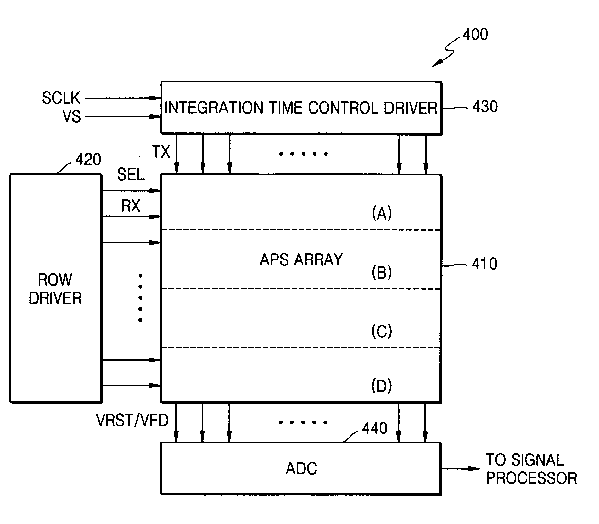
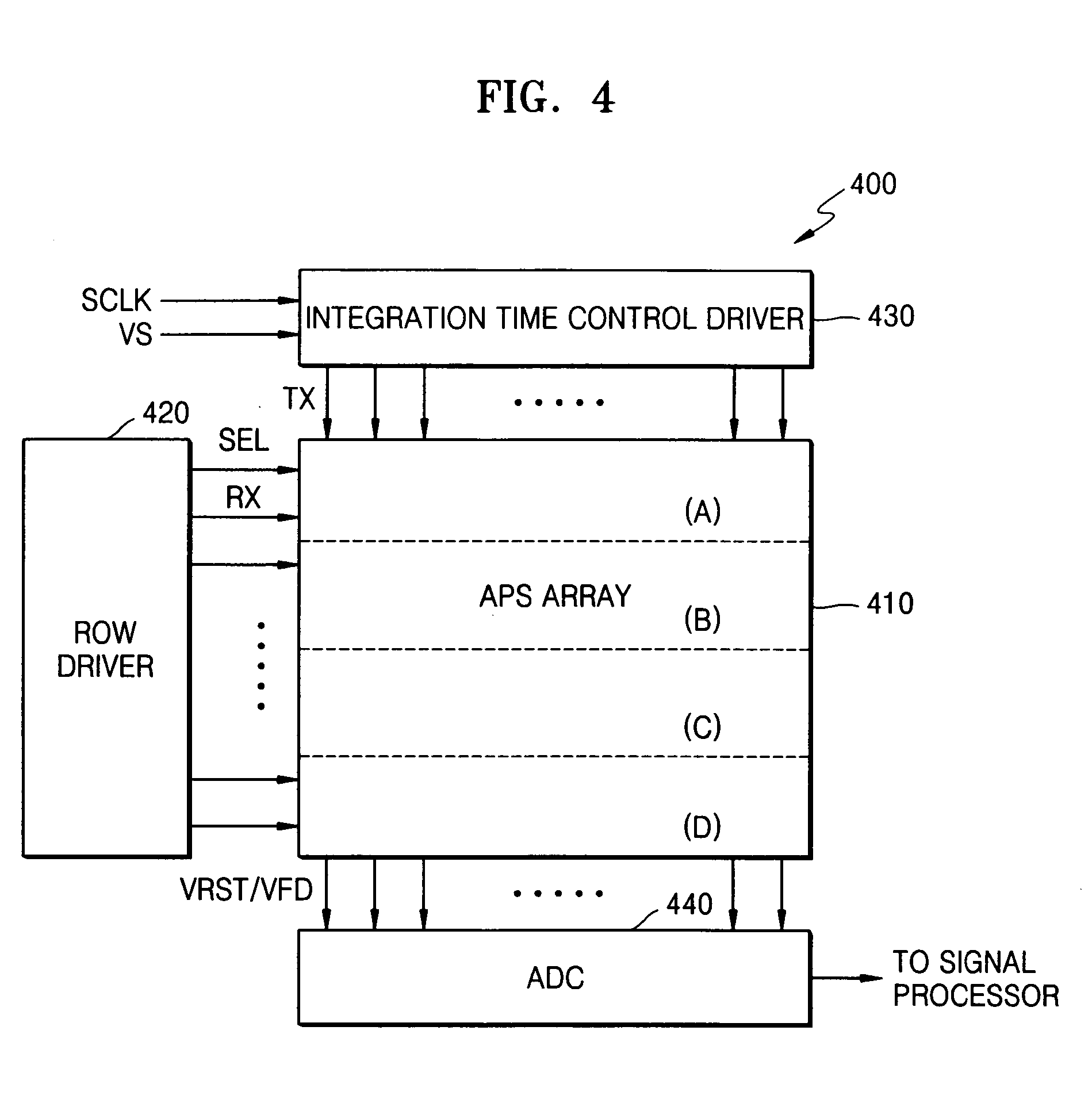
[0026]FIG. 4 is a block diagram of a complementary metal-oxide semiconductor (CMOS) image sensor (CIS)-type solid-state image-sensing device 400 according to an exemplary embodiment of the present invention. Referring to FIG. 4, the CIS-type solid-state image-sensing device 400 includes an active pixel sensor (APS) array 410, a row driver 420, an integration time control driver 430, and an analog-digital converter 440.

[0027]The APS array 410 is a two-dimensional array of pixels. The pixels of the APS array 410 are each configured in a circuit as illustrated in FIG. 5. Referring to FIG. 5, a pixel of the APS array 410 outputs a photoelectrically converted image signal VFD generated by a photo diode PD in response to a transmission control signal TX in a row selected by a row selection signal SEL, and then generates and outputs a reset signal VRST in response to a reset signal RX.

[0028]As shown in FIG. 5, each pixel includes four metal-oxide semiconductor field-effect transistors (MOS...


PUM


Abstract

A solid-state image-sensing device that compensates for brightness at edges of a screen and a method of driving the device are provided. The solid-state image-sensing device comprises: an active pixel sensor (APS) array including pixels disposed in a two-dimensional matrix, each pixel for outputting a photoelectrically converted image signal generated by a photodiode in response to one of a plurality of transmission control signals transmitted to a selected row of the APS array, and for generating and outputting a reset signal in response to a reset control signal; a row driver for selecting a row of the APS array by generating row selection signals and for generating the reset control signal; an integration time control driver for generating the transmission control signals for setting non-uniform integration times of the photodiodes in each pixel; and an analog-digital converter for converting an analog signal corresponding to a difference between the image signal and the reset signal into a digital signal.

Description

CROSS-REFERENCE TO RELATED APPLICATION[0001]This application claims priority to Korean Patent Application No. 2004-8255, filed on Feb. 9, 2004, in the Korean Intellectual Property Office, the disclosure of which is incorporated herein in its entirety by reference.FIELD OF THE INVENTION[0002]The present invention relates to a solid-state image-sensing device, and more particularly, to a complementary metal-oxide semiconductor (CMOS) image sensor (CIS)-type solid-state image-sensing device.DESCRIPTION OF THE RELATED ART[0003]A complementary metal-oxide semiconductor (CMOS) image sensor (CIS)-type solid-sate image-sensing device can be mounted in, for example, a mobile phone camera or digital still camera, and senses visible images, converts the images into electrical signals, and transfers the electrical signals to a digital signal processor. The digital signal processor processes color image data (e.g., red, green, and blue data) output from the solid-state image-sensing device, and ...

Claims


Application Information

Patent Timeline
Patent Type & Authority Patents(United States)
IPC IPC(8): H01L27/00H04N5/335H04N5/341H04N5/353H04N5/361H04N5/369H04N5/374H04N5/376H04N5/378H04N101/00
CPCH04N5/3535H04N5/374H04N5/3572H04N25/533H04N25/61H04N25/76F16H48/22F16H48/295
Inventor JANG, HYUN-JEONG
Owner SAMSUNG ELECTRONICS CO LTD
Why Eureka
Try Eureka