Eureka AIR delivers breakthrough ideas for toughest innovation challenges, trusted by R&D personnel around the world.

Liquid-crystal display device and method of fabricating the same

a liquid crystal display and display device technology, applied in non-linear optics, instruments, optics, etc., can solve the problems of low aperture ratio and achieve the effect of enhancing the aperture ratio of the active matrix type liquid crystal display device, widening the angle of vision, and low aperture ratio

Inactive Publication Date: 2002-01-24
SEMICON ENERGY LAB CO LTD
View PDF0 Cites 66 Cited by
  • Summary
  • Abstract
  • Description
  • Claims
  • Application Information

AI Technical Summary

Benefits of technology

[0009] Although an active matrix type liquid-crystal display device of IPS mode can widen the angle of vision, it has the disadvantage of low aperture ratio. The present invention provides means for solving such a problem, and has for its object to enhance the aperture ratio of the active matrix type liquid-crystal display device of IPS mode, thereby to realize an image display which has a wide angle of vision and which is clear and bright.

Problems solved by technology

Although an active matrix type liquid-crystal display device of IPS mode can widen the angle of vision, it has the disadvantage of low aperture ratio.

Method used

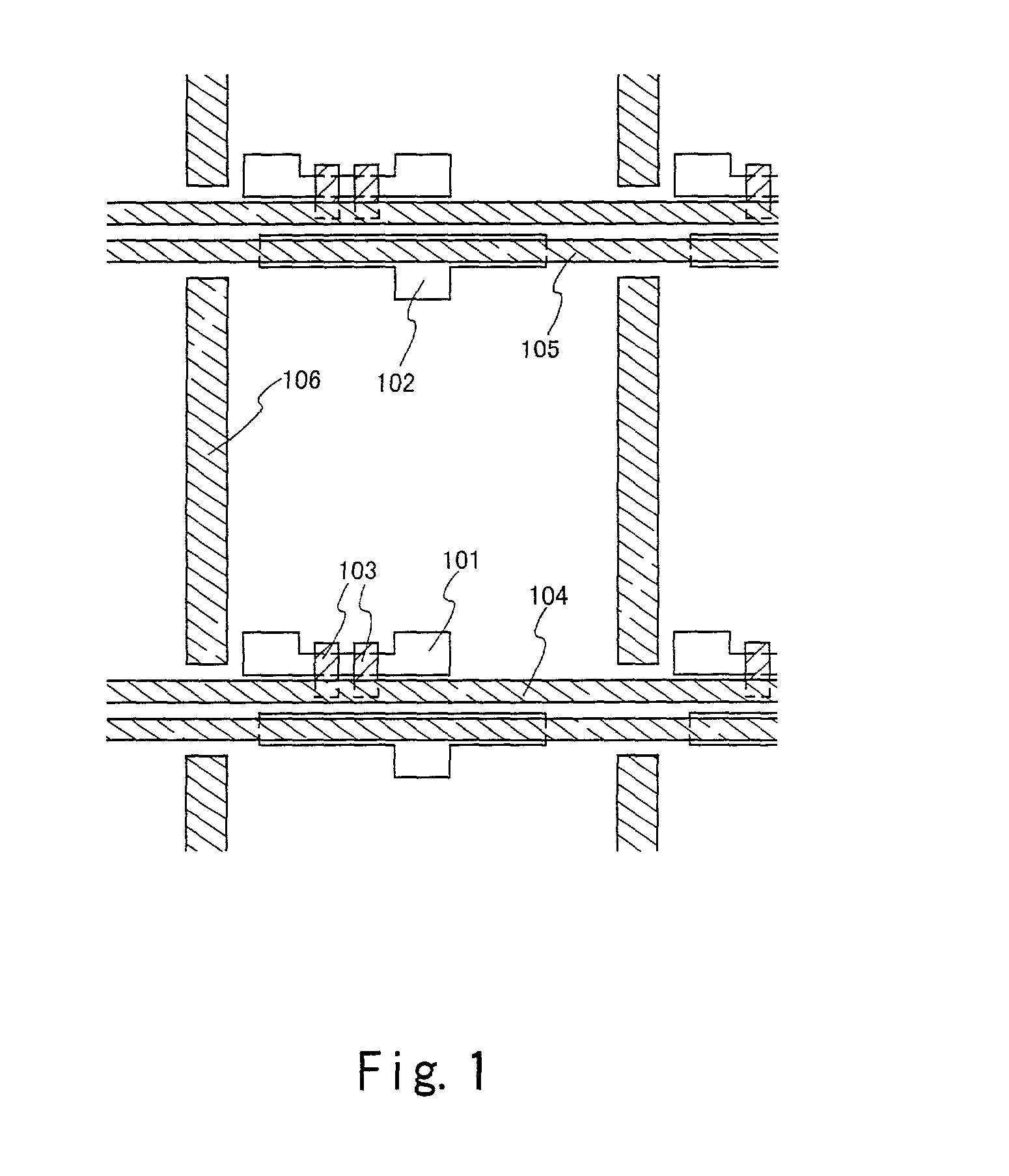
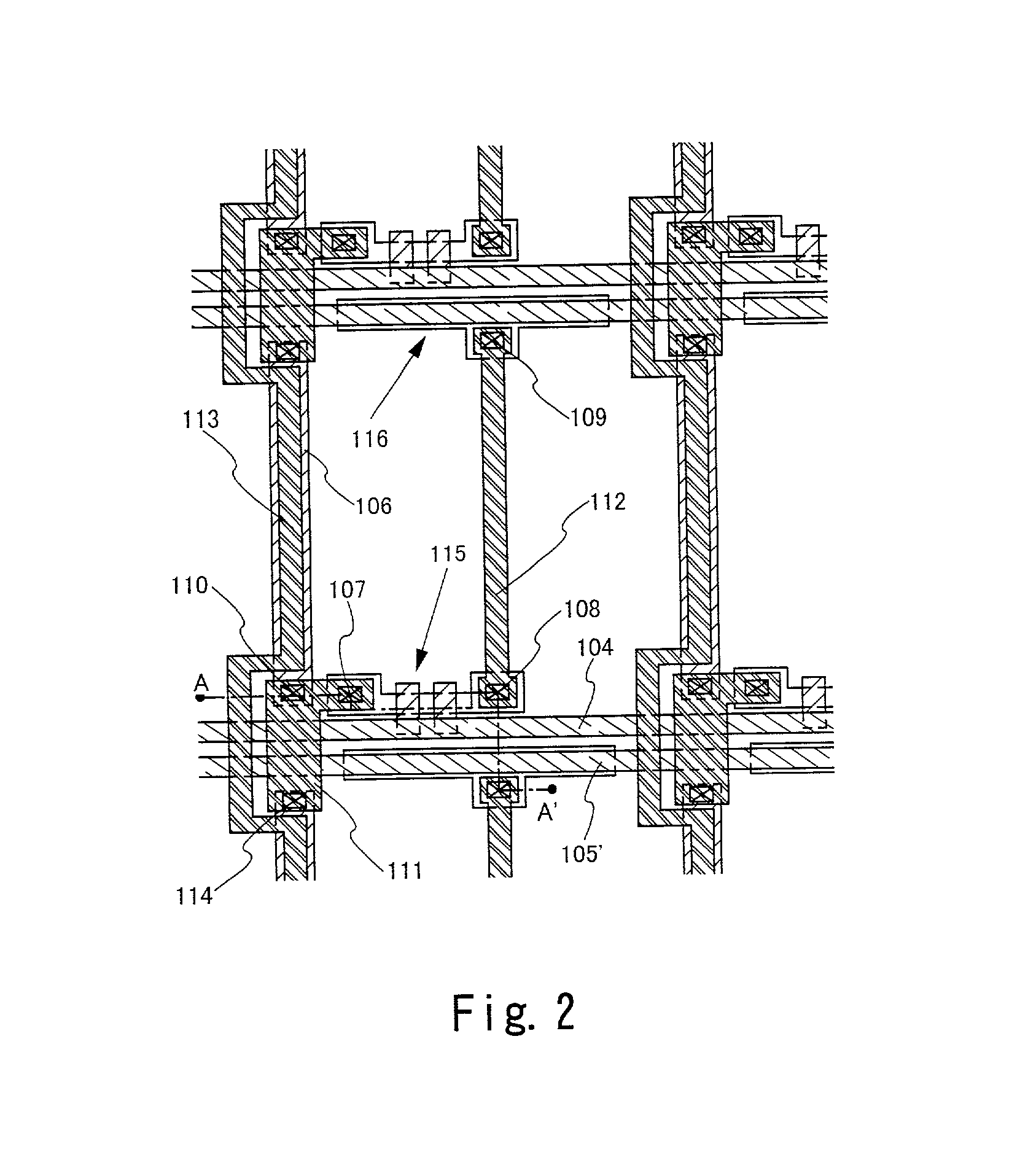
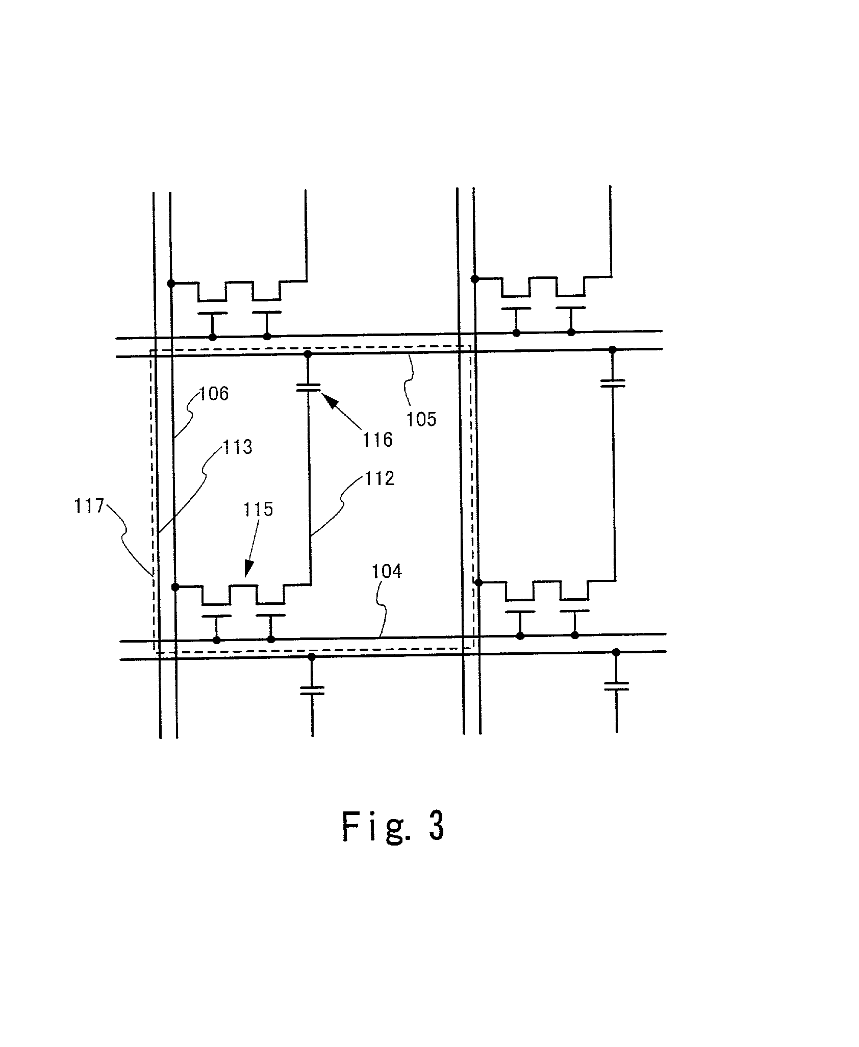

Image

  • Liquid-crystal display device and method of fabricating the same
  • Liquid-crystal display device and method of fabricating the same
  • Liquid-crystal display device and method of fabricating the same

Examples


embodiment 1

[0055] Embodiment 1

[0056] In this embodiment, there will be described in detail a method in which a pixel portion conforming to a pixel structure of IPS mode, and the TFTs of a driver circuit lying around the pixel portion are fabricated simultaneously.

[0057] The gate electrode of each of the TFTs mentioned in this embodiment has a double-layer structure. The first layer and second layer of the double-layer structure are both formed of an element which is selected from the group consisting of Ta, W, Ti and Mo, or an alloy material or compound material which contains the element as its main component. Alternatively, the first layer may well be formed of a semiconductor film which is typified by a polycrystal silicon film doped with an impurity element such as phosphorus. As an example of a preferable combination, the first layer is formed of Ta or tantalum nitride (TaN), or a stacked structure of tantalum nitride (TaN) and Ta, while the second layer is formed of W.

[0058] Although the...

embodiment 2

[0086] Embodiment 2

[0087] In this embodiment, there will be described a process for fabricating an active matrix type liquid-crystal display device from the active matrix substrate prepared in Embodiment 1. FIG. 9 shows a state where the active matrix substrate and a counter substrate 569 are stuck together. Initially, the active matrix substrate in the state of FIG. 8 is overlaid with an orientation film 567, which is subsequently subjected to rubbing. The counter substrate 569 is formed with color filter layers 570, 571, an overcoat layer 573, and an orientation film 574. The color filter layer 570 of red and the color filter layer 571 of blue are formed over the TFTs in a stacked state so as to serve also as a light shield film. Besides, the color filter layer 570 of red, the color filter layer 571 of blue and a color filter layer 572 of green are stacked in correspondence with the connecting electrode 560, so as to form a spacer. The color filter layer of each color is formed by...

embodiment 3

[0097] Embodiment 3

[0098] In this embodiment, another example in which the TFT structure of an active matrix substrate is different will be described with reference to FIG. 15.

[0099] The active matrix substrate shown in FIG. 15 is formed with a driver circuit 857 and a pixel portion 858. The driver circuit 857 includes a logic circuit unit 855 having a first p-channel TFT 850 and a first n-channel TFT 851, and a sampling circuit unit 856 having a second n-channel TFT 852. The pixel portion 858 includes a pixel TFT 853 and a storage capacitor 854. The TFTs of the logic circuit unit 855 of the driver circuit 857 form a shift register circuit, a buffer circuit, etc. The TFTs of the sampling circuit unit 856 are basically formed as analog switches.

[0100] The TFTs are formed in such a way that channel forming regions, source and drain regions, LDD regions, etc. are provided in insular semiconductor films 803-806 which overlap a subbing film 802 formed on a substrate 801. The subbing film...


PUM

PropertyMeasurementUnit
lengthaaaaaaaaaa
lengthaaaaaaaaaa
widthaaaaaaaaaa

Abstract

An active matrix type liquid-crystal display device of IPS mode has its aperture ratio enhanced, thereby to realize an image display which has a wide angle of vision and which is clear and bright. A pixel portion (in FIG. 2) in the liquid-crystal display device comprises a TFT (115) which includes a semiconductor film formed over a substrate, and gate electrodes formed on a first insulating layer, a gate wiring line (104) which is formed on the first insulating layer, a common wiring line (113) which crosses the gate wiring line (104) through a second insulating layer, a pixel electrode (112) which is formed on the second insulating layer and which is connected with the TFT (115) of the pixel portion, a signal wiring line (106) which is formed so as to underlie the common wiring line (113) through the second insulating layer, and a connecting electrode (111) which is formed on the second insulating layer. The pixel electrode (112) and the common wiring line (113) are arranged so as to generate an electric field parallel to the plane of the substrate, and the signal wiring line (106) and the semiconductor film are connected through the connecting electrode (111).

Description

BACKGROUND OF THE INVENTION[0001] 1. Field of the Invention[0002] The present invention relates to a liquid-crystal display device of active matrix type, and more particularly to an active matrix type liquid-crystal display device of IPS (In-Plane Switching) mode (horizontal electric field mode).[0003] 2. Description of the Related Art[0004] There has been known a liquid-crystal display device of active matrix type employing active elements such as thin film transistors (TFTs). The active matrix type liquid-crystal display device is capable of heightening a pixel density, and it is small in size and light in weight and is of low dissipation power, so that the monitor of a personal computer, the display panel of a liquid-crystal television set, and the like products have been developed as substitutes for CRTs. In particular, a technique in which the active layer of each TFT is formed of a film of crystalline semiconductor typified by polycrystal silicon, permits the switching TFTs of...

Claims


Application Information

Patent Timeline
Patent Type & Authority Applications(United States)
IPC IPC(8): G02F1/1343G02F1/1345
CPCG02F1/134363G02F1/1345
Inventor YAMAZAKI, SHUNPEIKOYAMA, JUN
Owner SEMICON ENERGY LAB CO LTD
Why Eureka
Eureka Blog
Learn More