Chip resistor and method of making the same

a chip resistor and resistor technology, applied in the direction of resistor details, resistors adapted for applying terminals, resistive material coating, etc., can solve the problem that the circuit using the chip resistor ab>1/b> may work improperly

Active Publication Date: 2006-10-31
ROHM CO LTD
View PDF6 Cites 24 Cited by
  • Summary
  • Abstract
  • Description
  • Claims
  • Application Information

AI Technical Summary

Benefits of technology

[0007]The present invention has been conceived under the above-described circumstances. Therefore, it is an object of the present invention to provide a chip resistor including insulating films which hardly come off a resistor element. Another subject of the present invention is to provide a method of making such a chip resistor.

Problems solved by technology

If the solder sticks to the lower surface 100a, the chip resistor A1 may exhibit a resistance which is different from an intended resistance, and an electric circuit using the chip resistor A1 may work improperly.

Method used


Image

  • Chip resistor and method of making the same
  • Chip resistor and method of making the same
  • Chip resistor and method of making the same

Examples


Embodiment Construction

[0031]A preferred embodiment of the present invention is specifically described below with reference to the accompanying drawings.

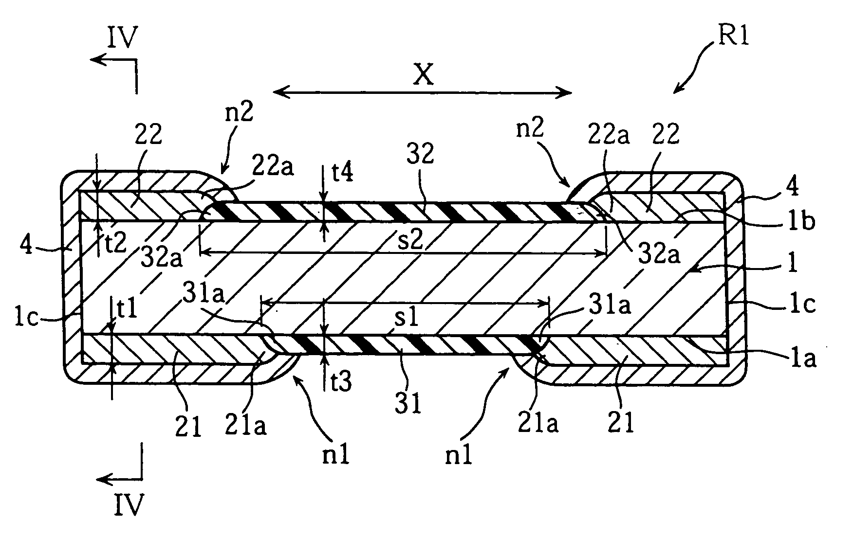
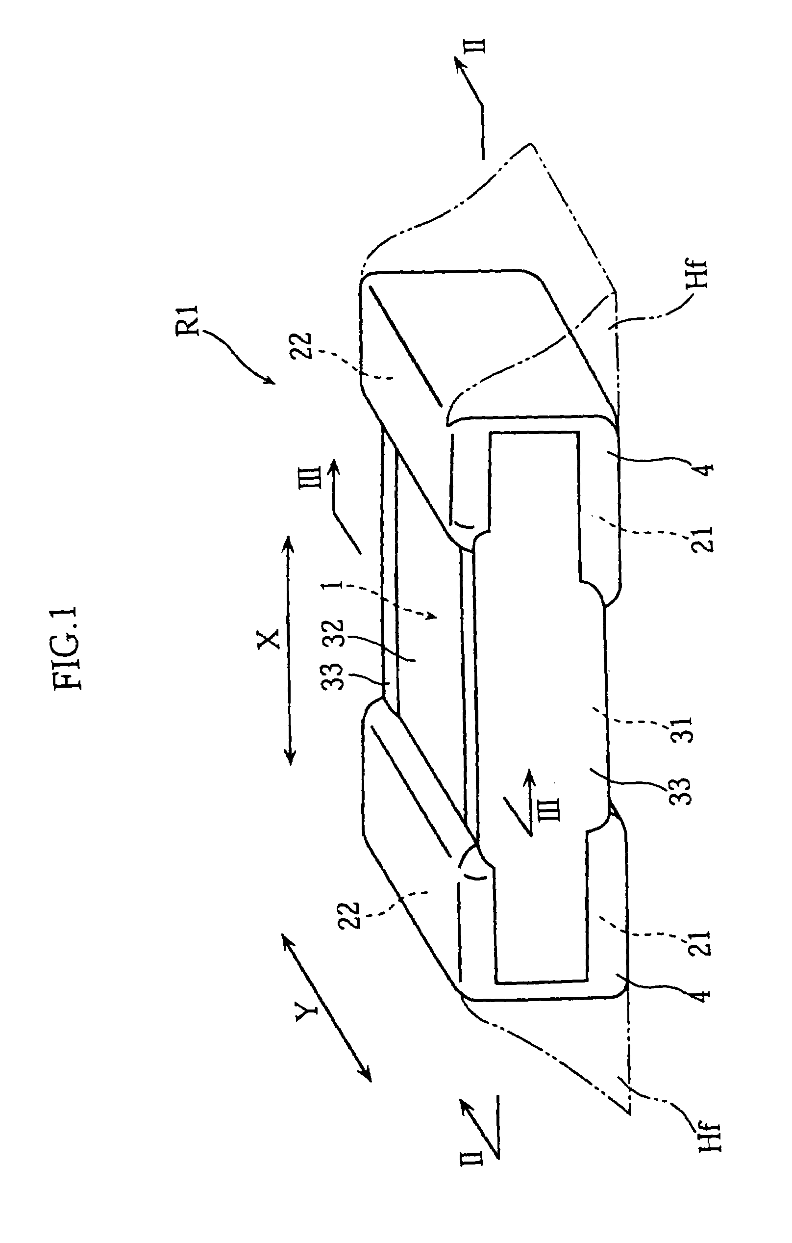
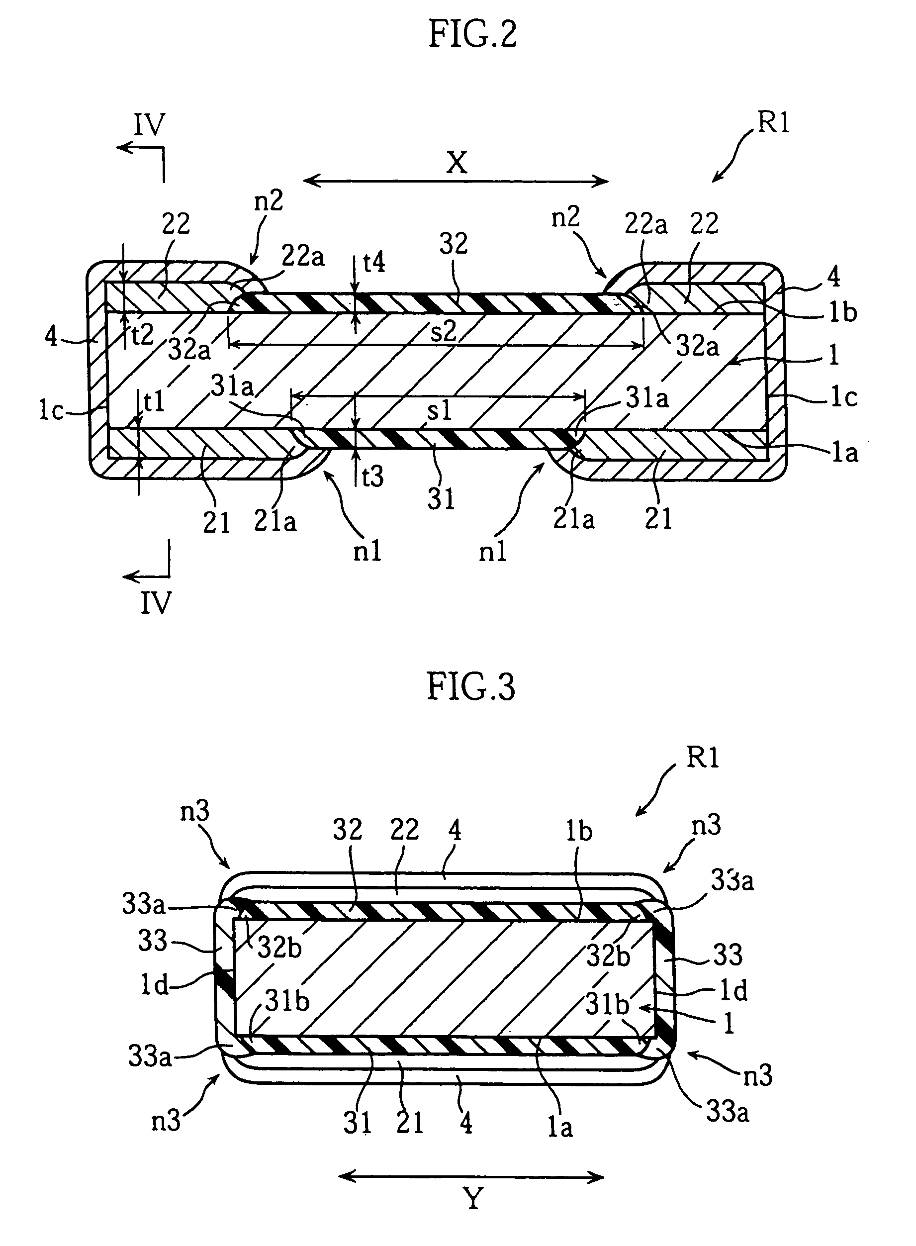
[0032]FIGS. 1 to 4 illustrate an example of a chip resistor according to the present invention. The illustrated chip resistor R1 includes a resistor element 1, a pair of main electrodes 21, a pair of auxiliary electrodes 22, first through third insulating films 31–33, and a pair of solder layers 4.

[0033]The resistor element 1 is a rectangular chip made of a metal and has a constant thickness as a whole. Examples of material include Ni—Cu alloy and Cu—Mn alloy. However, the material is not limitative on the present invention as long as the material has a resistivity suited to provide the chip resistor R1 with an intended resistance.

[0034]The pair of main electrodes 21 and the pair of auxiliary electrodes are made of the same material such as copper, for example. Each of the main electrodes 21 is formed on a lower surface 1a of the resistor element 1, while...


PUM

PropertyMeasurementUnit
thicknessaaaaaaaaaa
thicknessaaaaaaaaaa
thicknessaaaaaaaaaa

Abstract

A chip resistor includes a metal resistor element having a flat lower surface. The lower surface is formed with two electrodes spaced from each other, and an insulating resin film is formed between these electrodes. Each of the electrodes partially overlaps the insulating film so that a portion of the insulating film is inserted between each of the electrodes and the lower surface of the resistor element.

Description

BACKGROUND OF THE INVENTION[0001]1. Field of the Invention:[0002]The present invention relates to a chip resistor and a method of making the same.[0003]2. Description of Related Art:[0004]An example of conventional chip resistors is illustrated in FIG. 8 of the present application (refer to JP-A-2002-57009). A chip resistor A1 includes a metal chip resistor element 100 which has a lower surface 100a formed with a pair of electrodes 110. Each of the electrodes 110 includes a lower surface formed with a solder layer 120. As understood from the figure, the lower surface 100a of the resistor element includes two areas each covered with the electrode 110 and an exposed area between the electrodes.[0005]In use, the chip resistor A1 is soldered on a printed circuit board for example. It is desirable that molten solder sticks only to the two electrodes 110 of the chip resistor A1. However, according to the conventional structure shown in FIG. 8, molten solder may also stick to the above-des...

Claims


Application Information

Patent Timeline
Patent Type & Authority Patents(United States)
IPC IPC(8): H01C1/012H01C3/00H01C1/148H01C17/00H01C17/02H01C17/06H01C17/28
CPCH01C1/148H01C17/281H01C17/006Y10T29/49082
Inventor TSUKADA, TORAYUKI
Owner ROHM CO LTD
Why Eureka
Try Eureka