Analog modulation of optical signals

Inactive Publication Date: 2006-12-05
RPX CORP +1
10 Cites 16 Cited by

AI-Extracted Technical Summary

Problems solved by technology

This and other known optical signal modulation arrangements have limited bandwidth and, hence, there is a l...

Method used

[0019]FIG. 3 illustrates, in simplified block diagram form, a third embodiment of the invention. The embodiment of FIG. 3 is similar to that of FIG. 2 and includes similar elements that are essentially identical from both a physical and functional standpoint. These similar elements have been similarly numbers as those in FIG. 2 and will not be discussed again in detail. The only significant difference between the embodiments of FIG. 2 and FIG. 3 is how the sub-carrier modulated optical signal is generated in the embodiment of FIG. 3. As indicated above, there are several ways of generating the desired sub-carrier modulated optical signal upon which the data signal will eventually be modulated. In the embodiment of FIG. 3, a coherent technique is advantageously employed to realize the desired sub-carrier modulated optical signal. Specifically, in this example, two carrier optical signals are generated by employing tunable laser light sources 301 and 302. Signals for controlling the frequency (wavelengt...

Abstract

An optically modulated signal is generated for use in transporting data by generating a so-called sub-carrier modulated optical signal and, then, vector modulating the sub-carrier modulated optical signal to yield the desired modulated optical signal for transmission. The vector modulation includes a phase component and an amplitude component. In one specific embodiment of the invention, an apparatus for use in generating a modulated optical signal includes a generator to generate a sub-carrier modulated optical signal including an optical carrier and at least one sub-carrier and an analog vector modulator coupled to receive both the sub-carrier modulated optical signal from the generator and a data signal. The analog vector modulator generates an output optical signal by phase modulating and/or amplitude modulating the sub-carrier of the received optical signal in response to the data signal.

Application Domain

Time-division optical multiplex systemsWavelength-division multiplex systems +1

Technology Topic

SubcarrierPhase modulation +2

Image

  • Analog modulation of optical signals
  • Analog modulation of optical signals
  • Analog modulation of optical signals

Examples

  • Experimental program(2)

Example

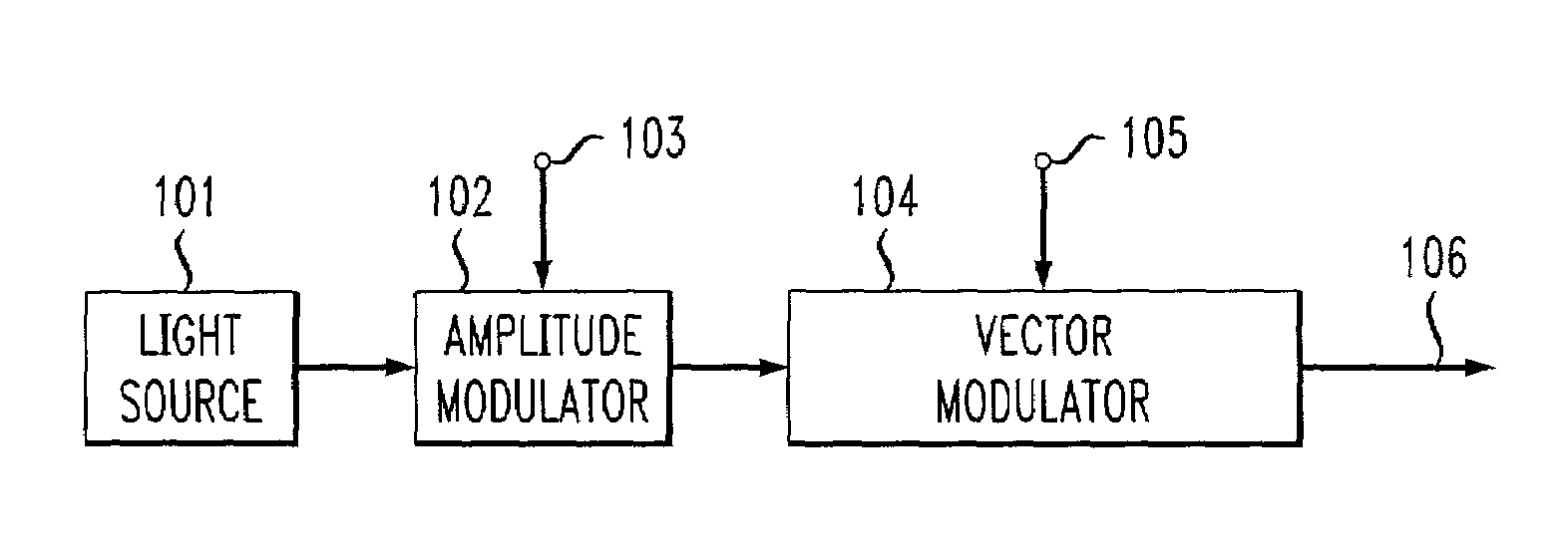
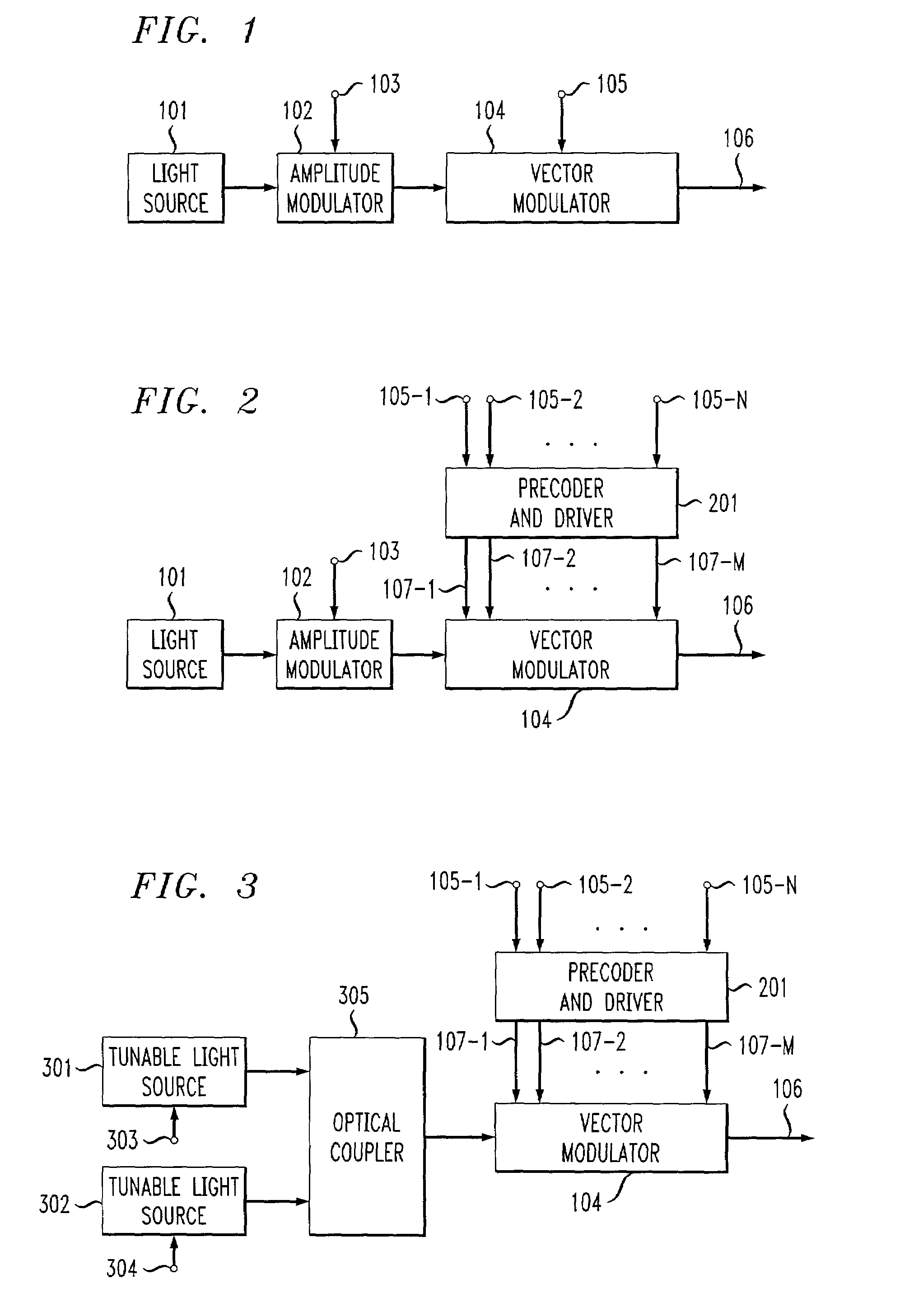
[0018]FIG. 2 also shows, in simplified block diagram form, a second embodiment of the invention. The embodiment of FIG. 2 is similar to that of FIG. 1 and includes similar elements that are essentially identical from both a physical and functional standpoint. These similar elements have been similarly numbers as those in FIG. 1 and will not be discussed again in detail. The only significant difference between the embodiments of FIG. 1 and FIG. 2 is the use of Precoder and Driver 201. As can be seen, one or more data signals are supplied to precoder and driver 201 via input connections 105-1 through 105-N. In precoder and driver 201, the data signals are employed to code and generate voltage signals for driving, phase modulators in vector modulator 104. These voltage signals are supplied via output connections 107-1 through 107-M to vector modulator 104. Again, details and operation of vector modulator 104 are described below regarding FIGS. 4 and 5 and a simple example of operation of precoder and driver 201 in conjunction with vector modulator 104 is described below regarding FIG. 7.

Example

[0019]FIG. 3 illustrates, in simplified block diagram form, a third embodiment of the invention. The embodiment of FIG. 3 is similar to that of FIG. 2 and includes similar elements that are essentially identical from both a physical and functional standpoint. These similar elements have been similarly numbers as those in FIG. 2 and will not be discussed again in detail. The only significant difference between the embodiments of FIG. 2 and FIG. 3 is how the sub-carrier modulated optical signal is generated in the embodiment of FIG. 3. As indicated above, there are several ways of generating the desired sub-carrier modulated optical signal upon which the data signal will eventually be modulated. In the embodiment of FIG. 3, a coherent technique is advantageously employed to realize the desired sub-carrier modulated optical signal. Specifically, in this example, two carrier optical signals are generated by employing tunable laser light sources 301 and 302. Signals for controlling the frequency (wavelength) of the laser light are supplied via connections 303 and 304 to tunable light sources 301 and 302, respectively. The resulting two optical carrier signals are tuned to have a prescribed wavelength offset and are overlaid coherently. At a receiving detector, typically a photodiode, the difference in wavelength generates a beating signal. The lasers, in this example, are single mode tunable lasers. This allows very wide tunability, since tuning the wavelength of one laser directly changes the frequency of the beating signal. Another advantage of using the two tunable lasers is that the resulting optical synthesizer generates a virtually harmonic free optical source. This results in an improved dynamic range and spurious free dynamic range of the optical link. Then, the two optical carriers that are offset relative to each other are supplied to optical coupler 305 where they are combined, i.e., mixed, to form the desired o sub-carrier modulated optical signal, which is supplied to vector modulator 104.
[0020]FIG. 4 shows, in simplified block diagram form, details of one vector modulator 104 that may be employed in the embodiments of the invention. The optical vector modulator 104 is based on the summing of multiple optical tapped delay lines. The principle of operation is as follows: The to be phase-shifted and/or to be amplitude-modulated signal could either be an amplitude-modulated single optical carrier generated by amplitude modulator 102 (FIG. 1 or FIG. 2) or include two optical carriers that are slightly offset in wavelength to generate a beating signal generated by tunable light sources 301 and 302 and coupler 305 of FIG. 3. This sub-carrier modulated optical signal is, when fed via 401 into the optical vector modulator 104 of FIG. 4, split into a plurality of similar branches by a power splitter 402, e.g., a multimode interference (MMI) coupler. Each branch is equipped with a phase modulator 403-1 through 403-M to adjust the phase of the optical carrier followed by an optical delay line. The delay in series with phase modulator 403-1, in this example, is zero (0). The delays in the remaining branches including phase modulators 403-2 through 403-M are generated by delay units 404-1 through 404-(M−1), respectively. Each of these delay lines in delay units 404-1 through 404-(M−1) changes the phase of the sub-carrier of the optical signal from phase modulators 403-2 through 403-M, respectively, by a fixed amount. For example, the delay line in unit 404-1 provides a delay of τ, delay unit 404-2 provides a delay of 2τ and delay unit 404-(M−1) provides a delay of (M−1)τ. Typically, a delay τ of 1/(M*sub-carrier frequency) is required. Thus, if the sub-carrier frequency is 40 GHz, the total delay range should be 0, . . . 25 picoseconds (ps). Another MMI coupler, i.e., power combiner 405, combines all of the phase-shifted and delayed optical signals from all branches to produce a modulated output optical signal at output 106, which will interfere constructively or destructively depending on the summing optical phases from all tributary branches. Therefore, by interfering signals with different carrier phase, the phase and the amplitude of the carrier of the summing signal can be set to an arbitrary state. These interfered optical carriers will produce microwave phasors with prescribed amplitude and phase at the remote optical detector.
[0021]The phase modulator 403 of each branch can be fabricated e.g. in a material system with linear electro-optic effect, as InP, GaAs or LiNbO3. The effective refractive index of an optical waveguide changes in proportion to the applied electrical field perpendicular to this waveguide. A high frequency distributed electrical waveguide is engineered to co-propagate with the optical wave with matched propagating velocity to deliver the local electrical field with high modulation bandwidth. The different branches will delay the optical signal by a different length of time. This results in different sub-carrier phases at the outputs of these delay lines in units 404. In the combiner 405, these different output signals that interfere constructively have a different sub-carrier phase due to the different time delays these signals experienced. The sub-carrier of the signal after the MMI coupler, i.e., power combiner 405, is the sum of all sub-carriers of the signals that interfere constructively.
[0022]FIG. 5 shows, in simplified block diagram form, details of a specific vector modulator that may be employed in the embodiments of the invention. Such an optical vector phase modulator 104 can be realized in a number of different configurations. One of the simplest designs is to use eight branches, which are grouped into pairs of two with the same delay line length. Basically, the branch pairs form Mach-Zehnder modulators 403. The delay lengths of these different pairs are designed such that they differ by a quarter period of the center frequency of the envelope signal. If now only one of the Mach-Zehnder structures is biased such that the optical signal of each arm interferes constructively, one can set four different phase states each separated by 90°. If two neighboring Mach Zehnder phase modulators 403 are switched on together, this results in a phase offset of 45° in comparison to the signal from a single Mach Zehnder phase modulator 403.
[0023]Specifically, FIG. 5 shows input 401 to which an appropriate sub-carrier modulated optical signal is supplied, for example, from amplitude modulator 102 of FIG. 2 or the two combined offset optical carriers generated by tunable light sources 301 and 302 and coupler 305 of FIG. 3. The supplied signal is split into eight branches and a branch is supplied to each one of phase modulators 403-1 through 403-8. Again, the phase modulators 403-1 through 403-8 are grouped into sets of two and each set has a different delay path. For example, a first set including phase modulators 403-1 and 403-2, has a zero delay; a second set including phase modulators 403-3 and 403-4, has a delay of τ generated by delay lines in delay units 501-1 and 501-2; a third set including phase modulators 403-5 and 403-6, has a delay of 2τ generated by delay lines in delay units 501-3 and 501-4; and a fourth set including phase modulators 403-7 and 403-8, has a delay of 3τ generated by delay lines in delay units 501-5 and 501-6. The optical signals from the eight branches are combined in power combiner 405 to yield the desired output optical signal at output 106.
[0024]FIG. 6 shows all possible phase/amplitude states of the optical envelope produced by vector modulator 104 of FIG. 5, if each phase modulator is driven either with 0V or with a Voltage that results in a π/2 phase shift of the optical carrier or with a Voltage that results in a π phase shift of the optical carrier. It is possible to use digital, multi-level or analog control signals, which allows obtaining all possible phase/amplitude states in-between the discrete ones shown in FIG. 6.
[0025]FIG. 7 illustrates, in simplified block diagram form, a simplified version of the invention to illustrate operation of the precoder and driver 201 shown in FIGS. 2 and 3. Specifically, optical light source 101 supplies an sub-carrier modulated optical signal to the vector modulator 104 and, therein, to power splitter 402. In this example, power splitter 402 splits the supplied optical carrier into three equal versions, i.e., branches, each of which is supplied to one of phase modulators 403-1, 403-2 and 403-3. An output of phase modulator 403-2 is supplied to delay unit 404-1 wherein a delay line delays the phase modulated signal by τ. An output of phase modulator 403-3 is supplied to delay unit 404-2 wherein a delay line delays the phase modulated signal by 2τ. In turn, the output from phase modulator 403-1 and the outputs from delay units 404-1 and 404-2 are supplied to power combiner 405 where they are combined, as described above, to generate the desired transport output optical signal at output 106. The transport optical signal is transmitted to a remote receiver where it is detected via, for example photodiode 701, which generates a desired signal at terminals 702. Returning, phase modulators 403-1, 403-2 and 403-2 are supplied control signals via paths 107-1, 107-2 and 107-3, respectively, from precoder and driver 201. The operation of precoder 201 can be explained by referring to the table in FIG. 8. In this example, it is desired to generate symbols A, B, C and D. This is realized by supplying a binary input to terminal 105-1 and 105-2 of precoder and driver 201. As seen in FIG. 9, the desired vectors corresponding to the location of the symbols A, B, C and D in the constellation shown in FIG. 9 are (0,0) 1<60°, (0,1) 1 <180° and (1,1) 0, respectively. These vectors are realized by controlling phase modulators 403-1, 403-2 and 403-3 by the modulation voltages V1, V2 and V3, respectively. Thus, for symbol A (binary input 0,0) V1=V2=V3=0, for symbol B (binary 0,1) V1=Vπ and V1=V2=0, for symbol C (binary 1,0) V1=V20 and V3=Vπ and for symbol D (binary 1,1) V1=V3=0 and V2=Vπ.
[0026]The above-described embodiments are, of course, merely illustrative of the principles of the invention. Indeed, numerous other methods or apparatus may be devised by those skilled in the art without departing from the spirit and scope of the invention.

PUM

no PUM

Description & Claims & Application Information

We can also present the details of the Description, Claims and Application information to help users get a comprehensive understanding of the technical details of the patent, such as background art, summary of invention, brief description of drawings, description of embodiments, and other original content. On the other hand, users can also determine the specific scope of protection of the technology through the list of claims; as well as understand the changes in the life cycle of the technology with the presentation of the patent timeline. Login to view more.
Why Eureka
Try Eureka