
MEMs device with feedback control

a technology of feedback control and ms device, which is applied in the direction of semiconductor devices, instruments, optics, etc., can solve the problems of snap-in snap-in form of electrostatic control and difficulty in fabrication

Active Publication Date: 2007-01-02
HEWLETT PACKARD DEV CO LP
View PDF8 Cites 20 Cited by
  • Summary
  • Abstract
  • Description
  • Claims
  • Application Information

AI Technical Summary

Benefits of technology

This solution enables precise and sensitive control of MEMS device movements, preventing stiction and snap-down, while maintaining compatibility with conventional manufacturing processes, allowing for maximum utilization of spatial working distance and minimizing electromechanical constraints.

Problems solved by technology

However, this form of electrostatic control has snap-in issues when the controllable gaps are reduced below a threshold limit.
Conventional devices incorporate mechanical stops to limit the gap displacement but these can be difficult to fabricate as there is often still some striction forces from the stops themselves.

Method used


Image

  • MEMs device with feedback control
  • MEMs device with feedback control
  • MEMs device with feedback control

Examples


Embodiment Construction

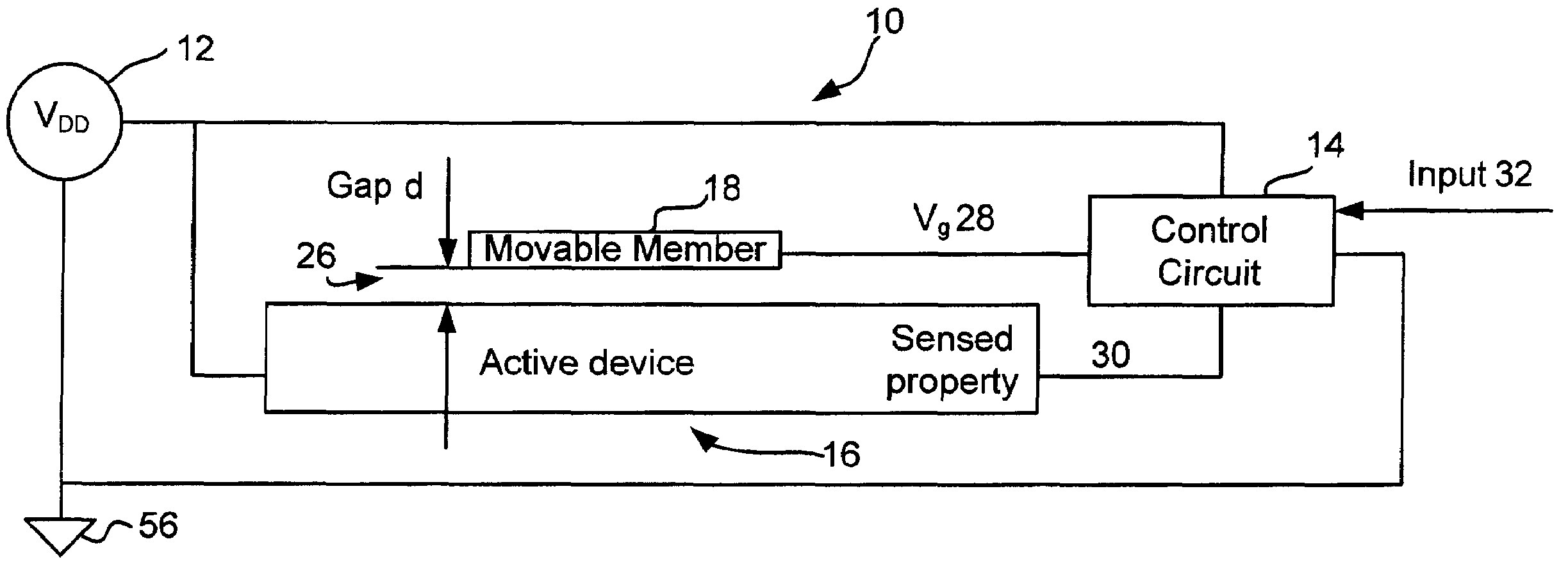
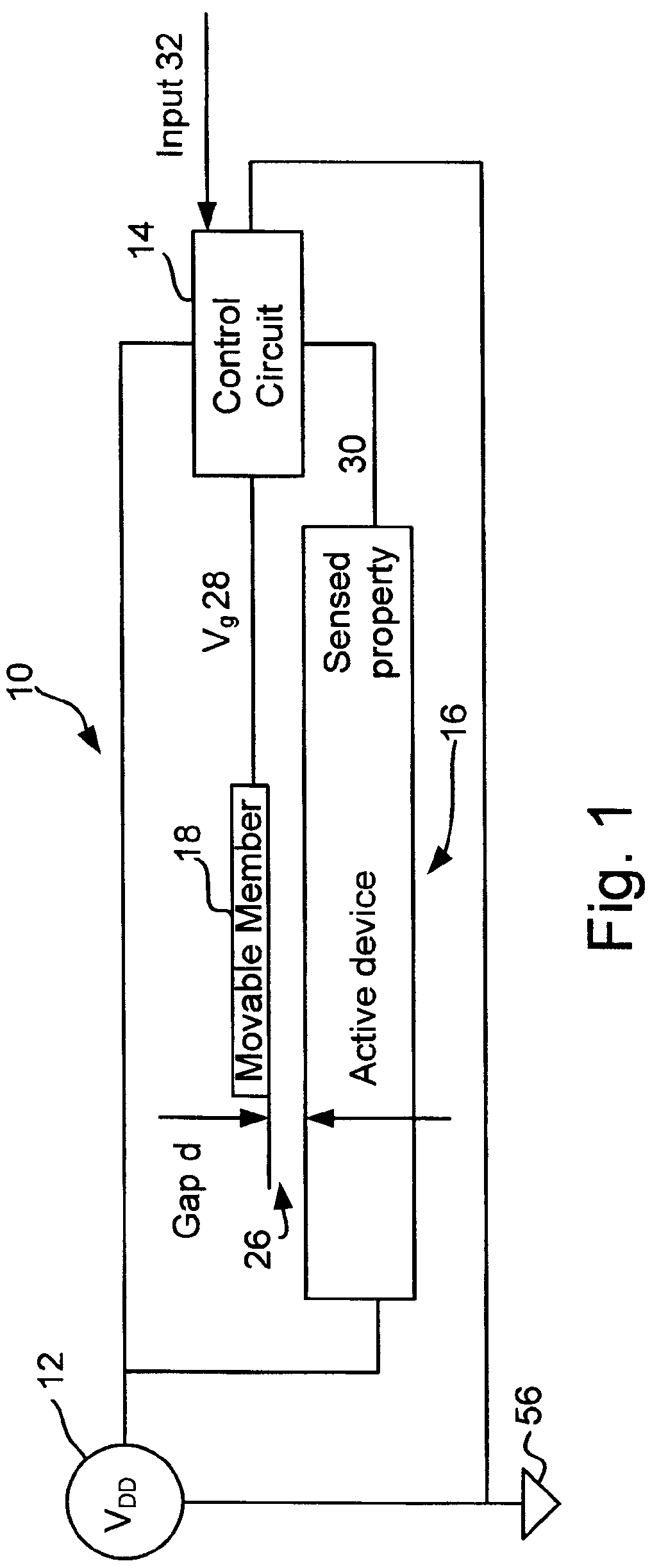
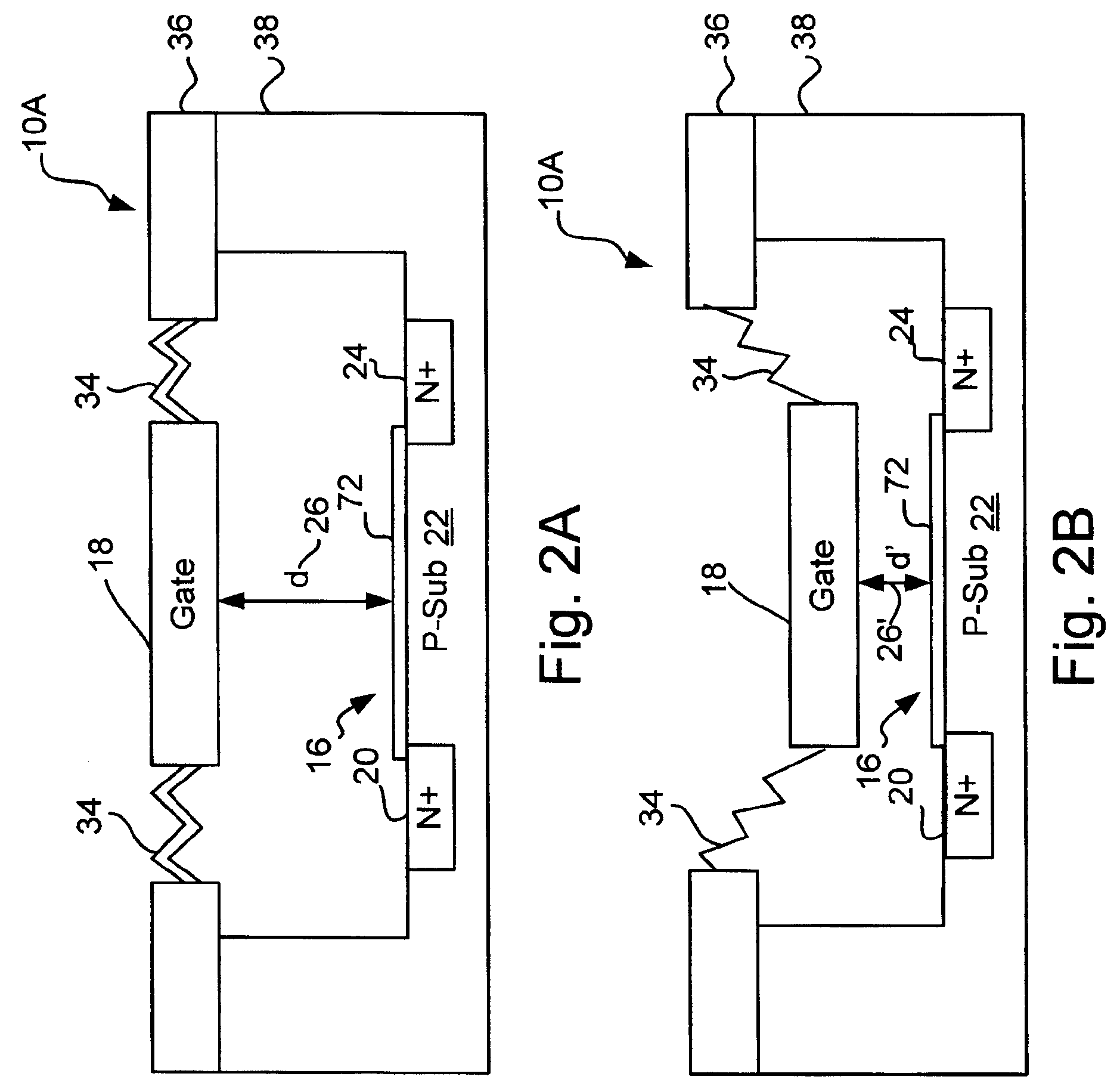
[0021]The MEMs devices of the present invention are applicable to a broad range of semiconductor, thin and thick film device technologies and can be fabricated from a variety of semiconductor technology related materials. The following description discusses several presently preferred embodiments of the MEMs and active devices of the present invention as implemented in silicon substrates, since the majority of currently available semiconductor devices are fabricated in silicon substrates and the most commonly encountered applications of the present invention will involve silicon substrates. Nevertheless, the present invention may also advantageously be employed in gallium arsenide, germanium, and other semiconductor materials. In addition, the present invention is not intended to be limited to those devices fabricated in silicon semiconductor materials, but will include those devices fabricated in one or more of the available MEMs and semiconductor related materials and technologies...


PUM


Abstract

A MEMS device includes at least one movable member and an active device having at least one property affected by the location of the movable member with respect to the active device. A control circuit is used to limit movement of the movable member based on observation of the property affected by the active device.

Description

CROSS-REFERENCE TO RELATED APPLICATIONS[0001]This application is a divisional of application Ser. No. 11 / 105,802, filed Apr. 13, 2005 now U.S. Pat. No. 7,061,660, hereby incorporated by reference.BACKGROUND OF THE INVENTION[0002]Electrostatic micro-electromechanical (MEMs) devices typically are fabricated with semiconductor or other thin and thick film technologies. The MEMs devices often times have electrostatic actuators that are used to control various functions in display devices, high precision position sensors, pressure sensors, voltage modulators, accelerometers, oscillators, and adaptive optics, just to name a few. Electrostatic actuation is generally performed using a constant voltage source as the implementation of the control is less complicated than other methods. However, this form of electrostatic control has snap-in issues when the controllable gaps are reduced below a threshold limit. Further, if a gap separates two different metal plates and the gap is removed by al...

Claims


Application Information

Patent Timeline
Patent Type & Authority Patents(United States)
IPC IPC(8): G02B26/00
CPCG02B26/001G02B26/0833G09G3/3433H01L31/0232G09G3/346G09G3/3466G09G2320/029G09G2320/0295G09G2360/147H01L31/02162G09G2300/0819
Inventor CHEN, ZHIZHANGLIAO, HANGRAMAMOORTHI, SRIRAMMYERS, TIMOTHY F.
Owner HEWLETT PACKARD DEV CO LP
Features
  • Generate Ideas
  • Intellectual Property
  • Life Sciences
  • Materials
  • Tech Scout
  • Unparalleled Data Quality
  • Higher Quality Content
  • 60% Fewer Hallucinations
Learn More