
Magnetic RAM and array architecture using a two transistor, one MTJ cell

a technology of array architecture and mtj cells, applied in the field of magnetic ram devices, can solve the problems of loss of data or change of switching threshold, significant disadvantage of adding a transistor to each cell, and the requirement for relatively large transistors

Active Publication Date: 2007-02-06
TAIWAN SEMICON MFG CO LTD
View PDF8 Cites 10 Cited by
  • Summary
  • Abstract
  • Description
  • Claims
  • Application Information

AI Technical Summary

Benefits of technology

The technical effect of this patent is to create a reliable and easy-to-manufacture magnetic RAM integrated circuit that works effectively.

Problems solved by technology

The technical problem addressed in this patent relates to improving the performance of Magneto-based random access memory (MRAM) arrays. Specifically, the patent discusses different methods for programming the magnetization direction in MRAM cells, including the use of a single crystal structure and multiple transistors. Additionally, the patent addresses issues related to cell interference and leakage caused by unconnected cells.

Method used


Image

  • Magnetic RAM and array architecture using a two transistor, one MTJ cell
  • Magnetic RAM and array architecture using a two transistor, one MTJ cell
  • Magnetic RAM and array architecture using a two transistor, one MTJ cell

Examples


Embodiment Construction

[0036]The preferred embodiments of the present invention disclose magnetic RAM devices. Methods of forming, programming, and reading magnetic RAM devices are disclosed. It should be clear to those experienced in the art that the present invention can be applied and extended without deviating from the scope of the present invention.

[0037]Referring now to FIG. 5, a preferred embodiment of the present invention is illustrated. Several important features of the present invention are shown and discussed below. A MTJ cell 150 is illustrated. The MTJ cell 150 comprises a pinned layer 154 and a free layer 160 separated by a dielectric layer 158. The pinned layer 154 and free layer 160 preferably comprise ferromagnetic materials that can be magnetized. The dielectric layer 158 preferably comprises an oxide layer. In addition, the dielectric layer 158 is made relatively thin so that it will conduct current by tunneling when a sufficiently large voltage is applied across the dielectric layer 1...


PUM


Abstract

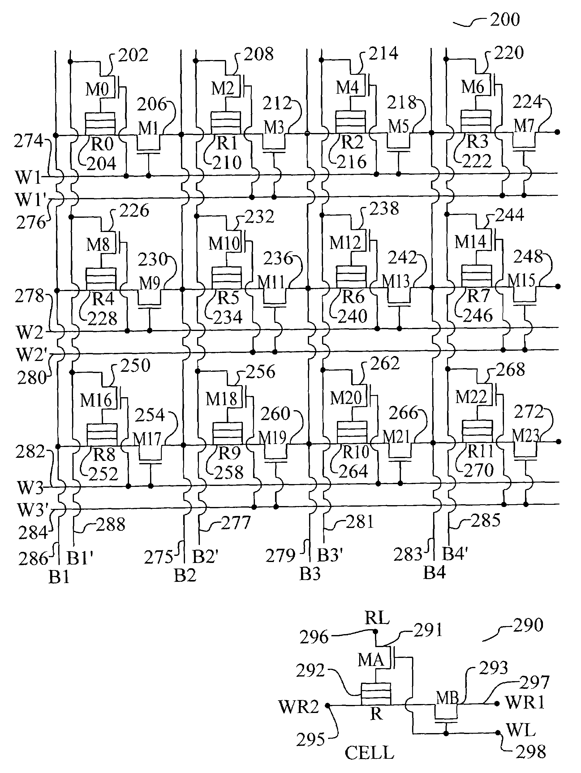
A new magnetic RAM cell device is achieved. The device comprisese, first, a MTJ cell comprising a free layer and a pinned layer separated by a dielectric layer. A reading switch is coupled between the free layer and a reading line. A writing switch is coupled between a first end of the pinned layer and a first writing line. A second end of the pinned layer is coupled to a second writing line. Architectures using MRAM cells are disclosed.

Description


Claims


Application Information

Patent Timeline
Owner TAIWAN SEMICON MFG CO LTD
Learn More