
Semiconductor memory device and magnetic ram device

A random access memory and storage device technology, applied in semiconductor devices, semiconductor/solid-state device parts, static memory, etc., can solve the problems of electromigration damage of programmable wires, eliminate electromigration, and improve reliability , Improving the effect of high current interconnect structures

Active Publication Date: 2007-06-27
TAIWAN SEMICON MFG CO LTD
View PDF0 Cites 2 Cited by
  • Summary
  • Abstract
  • Description
  • Claims
  • Application Information

AI Technical Summary

Problems solved by technology

High-current programmable wires of semiconductor memory devices are particularly compromised for electromigration

Method used


Image

  • Semiconductor memory device and magnetic ram device
  • Semiconductor memory device and magnetic ram device
  • Semiconductor memory device and magnetic ram device

Examples


Embodiment Construction

[0042] In the following description, several structures with new "short length" high current interconnects will be presented which improve the performance and reliability of integrated circuit (IC) programming.

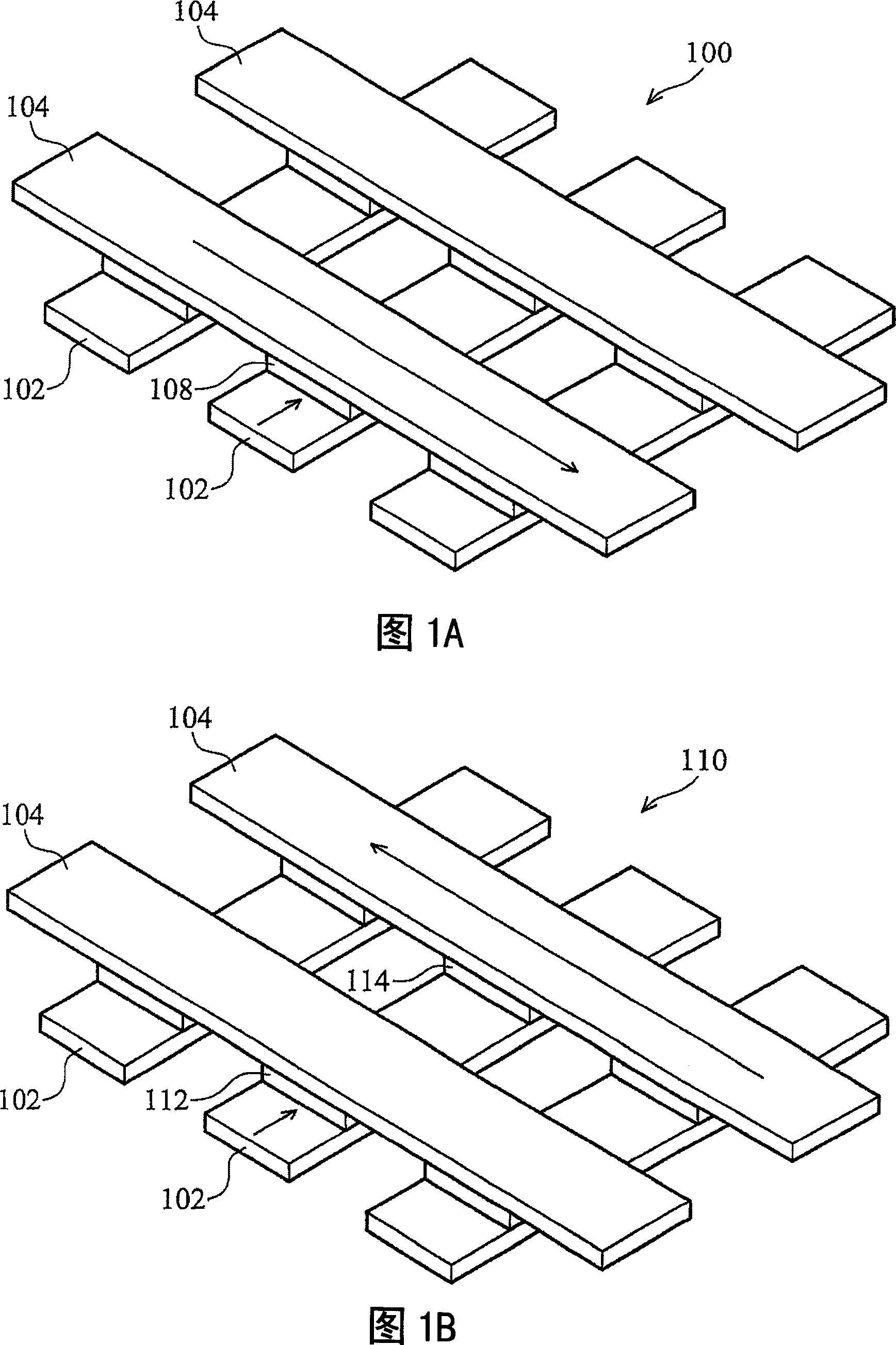
[0043] 1A and 1B illustrate two general Magnetic Random Access Memory (MRAM) memory cell layouts 100 and 110 . MRAM devices are non-volatile memories. Unlike DRAM chips, when programming is done using high currents, the data does not need to be continuously updated. In the future, due to the extremely low power consumption of MRAM, it is expected to use MRAM devices to replace DRAM and flash memory devices.

[0044] The MRAM memory cell layout 100 includes an interleaved plurality of word lines (columns) and a plurality of bit lines (rows). A plurality of MRAM memory cells are arranged at intersections of word lines and bit lines. The principles governing the operation of memory cells in MRAM are changes in the resistivity and thin-film structure of certain materia...


PUM


Abstract

The invention relates to a semiconductor memory device which is programmed by dualism of carrying characteristic of current passed through an adjacent memory cell. The semiconductor memory device includes a programmable memory cell and at least two current carrying structures. Wherein, at least one of the current carrying structures has a segmented current carrying structure comprising a plurality of first segments positioned on a first plane, the plurality of first segments is coupled with a plurality of second segments positioned on a second plane, and widths of the second segments are larger than the widths of the first segments. The semiconductor memory device of the invention improve a high current interconnection structure, eliminates an electron shift effect due to a high current density so as to enhance reliability.

Description

technical field [0001] The invention relates to a semiconductor storage device, in particular to a semiconductor storage device and a magnetic random access memory device with a high-current interconnection structure which are suitable for programming the integrated circuit storage device. Background technique [0002] Programmable semiconductor devices, such as dynamic random access memory (DRAM), flash memory, and magnetic random access memory (MRAM), generally require high current pulses to be properly programmed. Thus, wide interconnect wires are required to carry high currents to program these memory devices. In the past, wide wires did not cause problems with semiconductor geometries. Today, however, more and more smaller geometries are entering the sub-micron realm, causing designers to investigate every aspect of integrated circuit (IC) design to achieve these smaller and smaller geometries. This study also included wide interconnect high current wires in ICs used ...

Claims


Application Information

Patent Timeline
Patent Type & Authority Applications(China)
IPC IPC(8): H01L27/108H01L27/22H01L23/522G11C11/02H10B12/00
CPCH01L27/222H10B61/00
Inventor 欧东尼邓端理
Owner TAIWAN SEMICON MFG CO LTD
Learn More