Magnetic random access storage
A technology of random access memory and memory, applied in static memory, digital memory information, information storage, etc., to achieve the effect of reducing complexity and simplifying the unit structure
- Summary
- Abstract
- Description
- Claims
- Application Information
AI Technical Summary
Problems solved by technology
Method used
Image
Examples
Embodiment 1
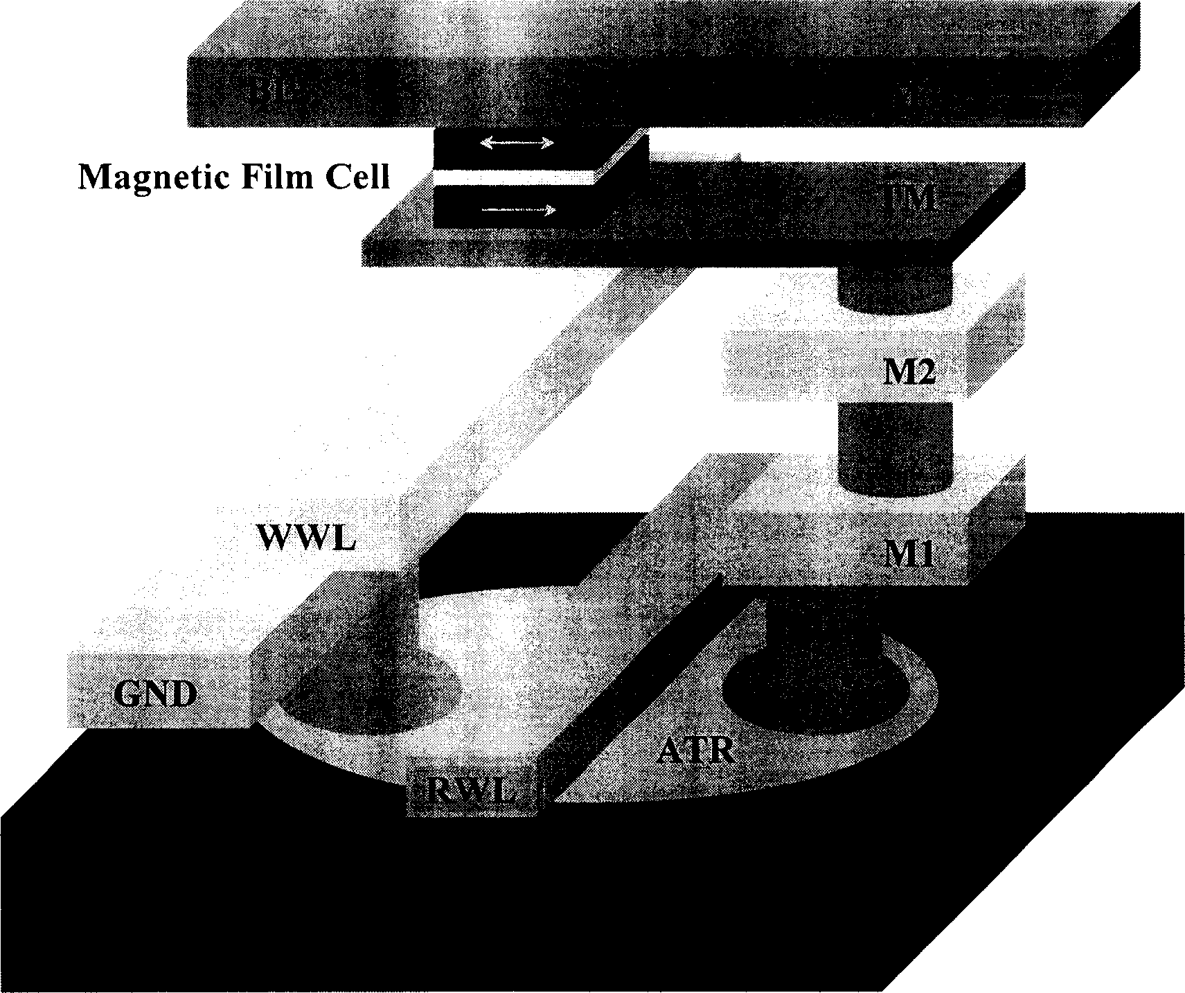
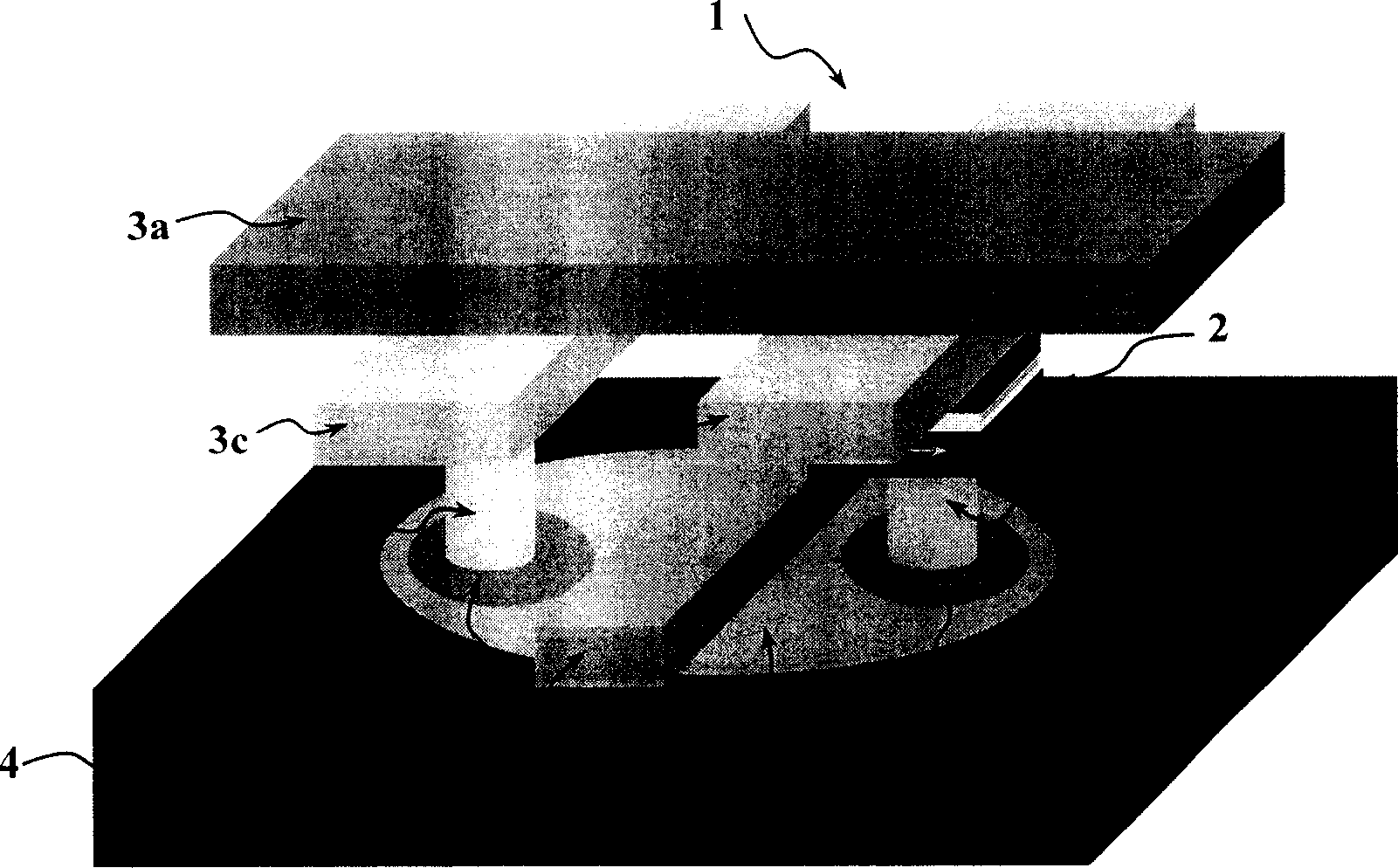
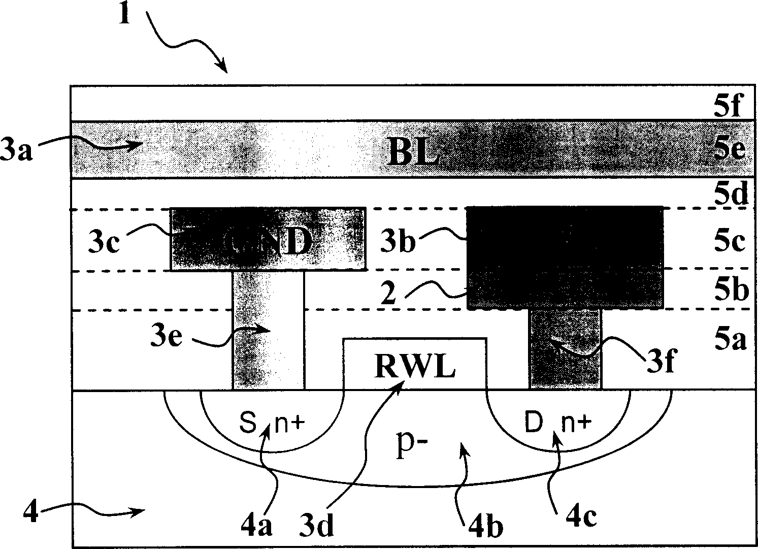
[0033] Such as figure 2 As shown, the magnetic thin film memory cell array in the MRAM memory is composed of a large number of MRAM cells 1, and one MRAM cell 1 includes a magnetic thin film memory cell 2, a transistor ATR 4 and a set of wiring, namely: bit line BL 3a, write word line WWL 3b, ground line GND 3c, read word line RWL 3d, and contact holes 3e, 3f for interlayer connection. Wherein, the bit line BL 3a and the writing word line WWL 3b are arranged above the magnetic thin film memory cell 2 in the layout, and the bit line BL 3a and the writing word line WWL 3b are in a right-angle relationship with each other in the vertical projection.
[0034] Such as image 3 As shown, the entire MRAM cell 1 is composed of several layers 5a, 5b, 5c, 5d, 5e, 5f in which non-functional areas are buried by an insulating buried medium. The metal wiring layer in the MRAM unit 1 has only two layers 5c and 5e, that is, the layer 5e where the bit line BL 3a is located and the layer 5c ...
Embodiment 2
[0036] Such as Figure 4 , Figure 5 As shown, it is a modification of Embodiment 1, in which a transition metal layer 3g is added, so that the magnetic thin film storage unit 2 can be arranged outside the area of the transistor ATR 4 in the vertical projection.
[0037] The magnetic thin-film memory cell array in the MRAM memory is composed of a large number of MRAM cells 1. In one MRAM cell 1, it includes a magnetic thin-film memory cell 2, a transistor ATR 4 and a set of wiring, namely: bit line BL 3a, write word line WWL 3b, ground line GND 3c, read word line RWL 3d, and contact holes 3e, 3f for interlayer connection and transition metal layer 3g. Wherein, the bit line BL 3a and the writing word line WWL 3b are arranged above the magnetic thin film memory cell 2 in the layout, and the bit line BL 3a and the writing word line WWL 3b are in a right-angle relationship with each other in the vertical projection.
[0038] The magnetic thin film memory cell 2 is arranged bel...
Embodiment 3
[0041] Such as Figure 6 As shown, the magnetic thin film memory cell array in the MRAM memory is composed of a large number of MRAM cells 1, and one MRAM cell 1 includes two magnetic thin film memory cells 2a, 2b, transistor ATR 4 and a set of wiring, namely: Bit line BL 3a, write word line WWL 3b, 3i, ground line GND 3c, read word line RWL 3d, 3j, and contact holes 3e, 3f, 3h for interlayer connection. In the layout, the bit line BL 3a and the writing word lines WWL 3b, 3i are arranged above the magnetic thin film memory cells 2a, 2b, and in the vertical projection, the bit line BL 3a and the writing word lines WWL 3b, 3i are in a right-angle relationship with each other.
[0042] The layout of this embodiment makes the two magnetic thin film storage units 2a, 2b share a ground line GND 3c, that is, the transistor ATR 4 units of two adjacent magnetic thin film storage units have a common source region 4a. Therefore, every two MRAM cells 1 can save the area of at least one...
PUM
 Abstract
Description
Claims
Application Information


