Resistor loading square ring ultra wide band wave absorbing structure

A square ring, ultra-wideband technology, applied in electrical components, magnetic field/electric field shielding, antennas, etc., can solve the problems of difficult outdoor environment, reflectivity can not meet application requirements, etc., to achieve simple unit structure, good wave absorption performance. Effect

Active Publication Date: 2022-03-18
CENT SOUTH UNIV
View PDF12 Cites 0 Cited by
  • Summary
  • Abstract
  • Description
  • Claims
  • Application Information

AI Technical Summary

Problems solved by technology

However, in practical applications, the reflectivity of -10dB cannot meet the application requirements of some scenarios, such as stealth technology, RCS reduction, electromagnetic compatibility design, etc.
Moreover, the functional layers of many current designs are exposed, so it is difficult to be used in outdoor environments, so it is of great significance to develop absorbing structures for more complex electromagnetic environments

Method used


Image

  • Resistor loading square ring ultra wide band wave absorbing structure
  • Resistor loading square ring ultra wide band wave absorbing structure
  • Resistor loading square ring ultra wide band wave absorbing structure

Examples


Embodiment 1

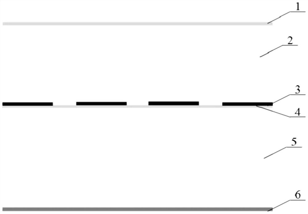
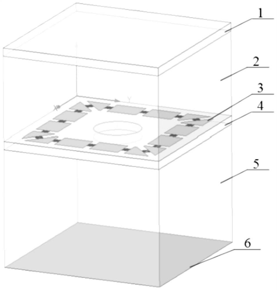
[0046] Schematic diagram of the cross-sectional structure of the resistance-loaded square ring ultra-broadband wave-absorbing structure of the present invention, as figure 1 As shown, from top to bottom are: surface skin dielectric layer 1, impedance matching dielectric layer 2, resistance-loaded square ring functional layer 3, functional layer substrate 4, structural support dielectric layer 5 and conductive reflective layer 6.

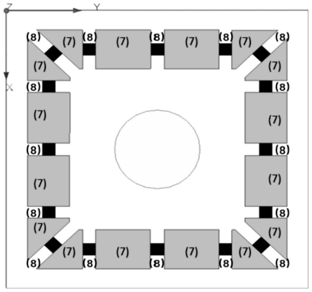
[0047] The schematic diagram of the structure unit of the resistance-loaded square ring ultra-broadband absorbing structure is as follows: figure 2 As shown, a circular hole is opened in the center of the functional layer substrate 4; the resistance-loaded square ring functional layer 3 is a square ring circuit formed by connecting a conductive square plate 7 and a resistor 8, and its specific structure can be seen image 3 , a single square ring loop includes 12 conductive square plates 7 and 16 resistors 8; two conductive square plates 7 are arra...


PUM

PropertyMeasurementUnit
Thicknessaaaaaaaaaa
Thicknessaaaaaaaaaa
Lengthaaaaaaaaaa

Abstract

The invention discloses a resistance loading square ring ultra-wideband wave-absorbing structure which comprises a surface skin dielectric layer, an impedance matching dielectric layer, a resistance loading square ring functional layer, a functional layer substrate, a structure supporting dielectric and a conductive reflecting layer which are sequentially arranged from top to bottom. The resistor loading square ring functional layer is composed of N * N square ring loops, each square ring loop is composed of a plurality of conductive square plates and a plurality of resistors, the conductive square plates are connected through the resistors to form a closed loop of the square rings, and the conductive square plates and the resistors are evenly distributed on the loop. The resistor loading square ring ultra-wideband wave-absorbing structure is simple in structure, wide in wave-absorbing frequency band and efficient in wave-absorbing performance, ultra-wideband high-performance electromagnetic wave absorption can be achieved, and the resistor loading square ring ultra-wideband wave-absorbing structure has wide application prospects in the fields of stealth technology, RCS reduction, electromagnetic compatibility design and the like.

Description

technical field [0001] The invention relates to the technical field of electromagnetic wave absorption, in particular to a resistance-loaded square-ring ultra-broadband wave-absorbing structure. Background technique [0002] Absorbing structures have extensive and profound application requirements in modern application scenarios, such as avoiding signal interference in similar frequency bands of multiple signal transmission systems in electronic equipment, reducing the scattering cross section of radar antennas, and stealth technology. [0003] Salisbury screens and Jaumann absorbers are earlier traditional absorbing structures with single (Salisbury) or multiple (Jaumann) resistive layers. However, the absorption band of the Salisbury screen is relatively narrow, and Jaumann increased the thickness of the absorbing structure while expanding the bandwidth. To achieve thin broadband absorption, Munk proposed circuit-analog (CA) absorbing structures based on frequency-selecti...

Claims


Application Information

Patent Timeline
IPC IPC(8): H01Q17/00H05K9/00
CPCH01Q17/008H05K9/0088
Inventor 姜超麻晢乂培
Owner CENT SOUTH UNIV
Why Eureka
Try Eureka