An active integrated structure of non-volatile resistive variable memory

A resistive memory, non-volatile technology, applied in the storage field, can solve the problems of large operating current, slow erasing and writing speed, and difficulty in reducing the size of the device, and achieves the effect of reducing the manufacturing cost and simplifying the structural unit of the integrated device.

Inactive Publication Date: 2018-03-16
SUN YAT SEN UNIV
View PDF4 Cites 0 Cited by
  • Summary
  • Abstract
  • Description
  • Claims
  • Application Information

AI Technical Summary

Problems solved by technology

[0003] At present, the mainstream non-volatile memory in the market is flash memory based on the charge storage mechanism. However, due to its large operating current, slow erasing and writing speed, high durability, high writing voltage, and device size, it is difficult to shrink to below 22 nanometers. and other shortcomings can no longer meet the needs of the rapid development of the electronic information technology industry

Method used


Image

  • An active integrated structure of non-volatile resistive variable memory
  • An active integrated structure of non-volatile resistive variable memory
  • An active integrated structure of non-volatile resistive variable memory

Examples


Embodiment 1

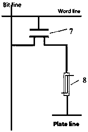
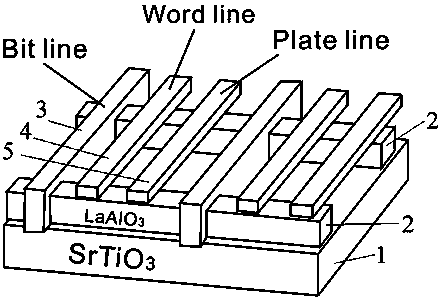
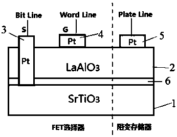
[0028] like figure 2 and image 3 As shown, the active integrated structure of the non-volatile resistive memory of the present invention specifically includes SrTiO 3 Substrate 1, set on SrTiO 3 LaAlO on substrate 1 3 Thin films 2 and located on SrTiO 3 on substrate 1 and through LaAlO 3 The first metal electrode 3 of the thin film 2, the first metal electrode 3 serves as the source S and the bit line Bit line, LaAlO 3 The thin film 2 is provided with the second metal electrode 4 as the gate G and the word line Word line and the third metal electrode 5 as the plate line Plate line, SrTiO 3 Substrate 1 with LaAlO 3 A two-dimensional electron gas 6 is formed between the interfaces of the thin films 2 .

[0029] The first metal electrode 3, the second metal electrode 4 and the third metal electrode 5 are all platinum electrodes.

[0030] The structural expression of the memory realized by the present invention is: Pt / LaAlO 3 / SrTiO 3 , in this structure, the channel l...


PUM


Abstract

The invention relates to the field of storage technology, in particular to an active integrated structure of a non-volatile resistive variable memory. It comprises a SrTiO3 substrate, a LaAlO3 thin film disposed on the SrTiO3 substrate and a first metal electrode disposed on the SrTiO3 substrate and passing through the LaAlO3 thin film, the first metal electrode is used as a source S and a bit line, and the LaAlO3 thin film is provided with A two-dimensional electron gas is formed between the interface of the SrTiO3 substrate and the LaAlO3 thin film as the second metal electrode of the gate G and the word line and the third metal electrode as the plate line. The present invention connects the channel layer of the FET selector and the bottom electrode of the resistive variable memory through a two-dimensional electron gas, which can save the preparation of the FET drain electrode, and the LaAlO3 thin film can be used as the dielectric layer and the non-volatile resistor of the FET selector at the same time. The storage medium of the variable memory can greatly simplify the structural unit of the integrated device, reduce the manufacturing cost of the device intersecting array and the manufacturing process of the high-density intersecting array.

Description

technical field [0001] The present invention relates to the field of storage technology, in particular, to a non-volatile resistive memory active integrated structure. Background technique [0002] Non-volatile memory has the advantage that the logic data stored in the device can still be stored for a long time without power supply. It is one of the most important hardware in digital information technology, and has attracted the attention of scholars and enterprises. [0003] At present, the mainstream non-volatile memory on the market is flash memory based on a charge storage mechanism. However, due to its large operating current, slow erasing and writing speed, high durability, high writing voltage, and device size, it is difficult to reduce the size of the device below 22 nanometers. Such shortcomings can no longer meet the needs of the rapid development of the electronic information technology industry. The development of a new next-generation information storage techno...

Claims


Application Information

Patent Timeline
Patent Type & Authority Patents(China)
IPC IPC(8): H01L27/24H01L45/00
Inventor 常雨诗吴曙翔李树玮
Owner SUN YAT SEN UNIV
Why Eureka
Try Eureka