Analog content addressable memory based on multi-stage flash memory transistor

A technology for addressing memory and transistors, applied in static memory, memory system, read-only memory, etc., can solve the problems of high power consumption and area overhead, low information storage density, complex circuit structure, etc., to improve storage density, simplify Cell structure, the effect of reducing the chip area

Pending Publication Date: 2022-05-13
ZHEJIANG UNIV
View PDF0 Cites 0 Cited by
  • Summary
  • Abstract
  • Description
  • Claims
  • Application Information

AI Technical Summary

Problems solved by technology

The third state of the tri-state content-addressable memory enables both exact match search and fuzzy match search to improve efficiency, but traditional content-addressable memory can only be used to search for a single determined data, There is still room for improvement
[0004] Although content-addressable memory cells and content-addressable memories based on static random access memory (SRAM), memristor (RRAM), magnetic memory (MRAM) and phase-change memory (PCM) have been realized or proposed, However, they have many defects such as (1) complex circuit structure, (2) complex timing logic, (3) high power consumption and area overhead, (4) adjacent cell interference, and (5) low information storage density.

Method used


Image

  • Analog content addressable memory based on multi-stage flash memory transistor
  • Analog content addressable memory based on multi-stage flash memory transistor
  • Analog content addressable memory based on multi-stage flash memory transistor

Examples


Embodiment Construction

[0033] The following introduces some of the possible embodiments of the present invention, which are intended to provide a basic understanding of the present invention, but are not intended to identify key or decisive elements of the present invention or limit the scope of protection. It is easy to understand that, according to the technical solution of the present invention, those skilled in the art may propose other alternative implementation manners without changing the essence and spirit of the present invention. Therefore, the following specific embodiments and drawings are only exemplary descriptions of the technical solution of the present invention, and should not be regarded as the entirety of the present invention or as a limitation or limitation on the technical solution of the present invention.

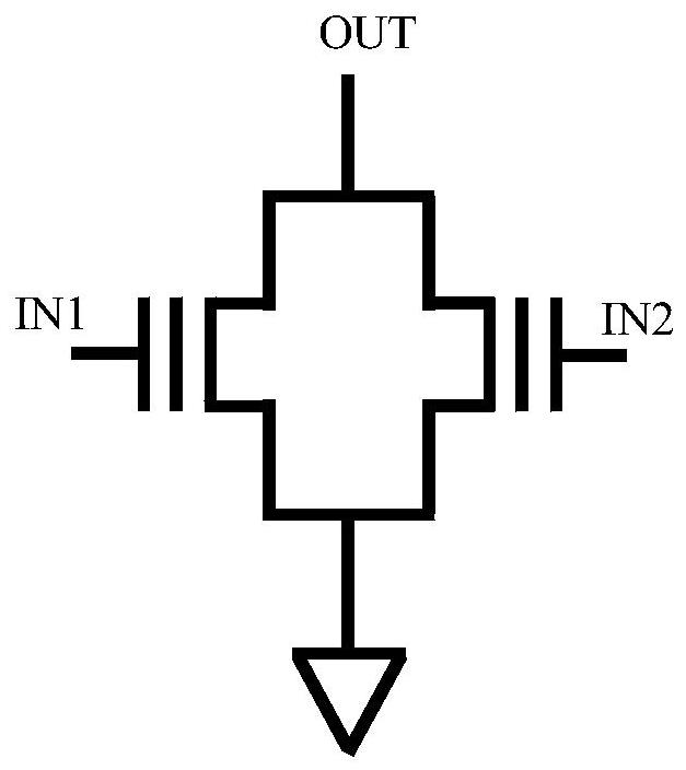
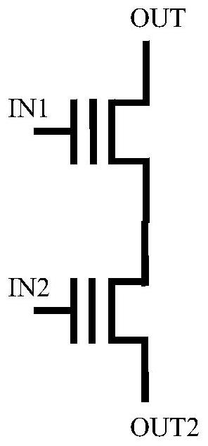
[0034] Each analog content addressable storage unit includes at least two multi-level flash memory transistors, at least two input ports, and at least one output port; the...


PUM


Abstract

The invention discloses an analog content addressable memory based on a multi-stage flash memory transistor. Each analog content addressable memory unit stores at least two pieces of multi-bit data, and range content searching of multi-bit input data can be carried out, that is, whether the input data is in a data range determined by the stored multi-bit data or not is searched; each analog content addressable memory unit comprises at least two multi-stage flash memory transistors, and the connection modes of the multi-stage flash memory transistors can be divided into a parallel connection mode and a series connection mode; the analog content addressable memory based on the multi-stage flash memory transistor can be composed of units in a parallel connection method or units in a series connection method, and range content searching and content addressing can be carried out on multiple pieces of multi-bit data at the same time. By adopting the nonvolatile flash memory, the static power consumption can be reduced, and the unit structure can be simplified; in addition, the innovative application of the multi-stage flash memory transistor is helpful for promoting the development of a storage technology, and has important significance for improving the performance of a memory.

Description

technical field [0001] The invention belongs to the field of semiconductors and integrated circuits, and in particular relates to an analog content addressable memory capable of performing range content search on analog data. Background technique [0002] At the core node of the router, the routing table is the most important concept, which stores the sending path determined by the destination IP in the data packet in the router. In the actual message forwarding process of the router, this is a method of finding the address based on the content. search process. There are many traditional search methods, such as wired search method, binary tree search method and hash table search method. These search methods are all search methods based on software algorithms, and the common feature is that the search speed is slow and the efficiency is low. Although there are many optimization methods for these search algorithms, it is still difficult to meet the high-speed search requirem...

Claims


Application Information

Patent Timeline
Patent Type & Authority Applications(China)
IPC IPC(8): G11C16/08G11C5/14G06F12/02
CPCG11C16/08G11C5/147G06F12/0238G06F12/0292
Inventor 赵毅杨帆高世凡
Owner ZHEJIANG UNIV
Why Eureka
Try Eureka