Magnetic RAM

a random access memory and magnetic technology, applied in the field of magnetic random access memory or mram, can solve the problems of soiling of the etch chamber, material etching by rie-type etching tends to be less reactive, and the material generally used to form the memory elements is little reactiv

Inactive Publication Date: 2006-07-06
STMICROELECTRONICS (ROUSSET) SAS
View PDF9 Cites 2 Cited by
  • Summary
  • Abstract
  • Description
  • Claims
  • Application Information

AI Technical Summary

Benefits of technology

[0022] According to an embodiment of the present invention, the first magnetic portion is connected to a source or drain region of a field-effect transistor.

Problems solved by technology

A disadvantage is that the materials generally used to form the memory elements are little reactive with the chemical etches conventionally used in integrated circuit manufacturing processes, since there is no forming of volatile compounds.
A disadvantage of such etchings is that the materials etched by an RIE-type etch tend to deposit back on the walls of the etch chamber and / or on other portions of the integrated circuit.
This may result in a soiling of the etch chamber, and / or, which is much more disturbing, the occurrence of defects at the integrated circuit level.

Method used


Image

  • Magnetic RAM
  • Magnetic RAM
  • Magnetic RAM

Examples


Embodiment Construction

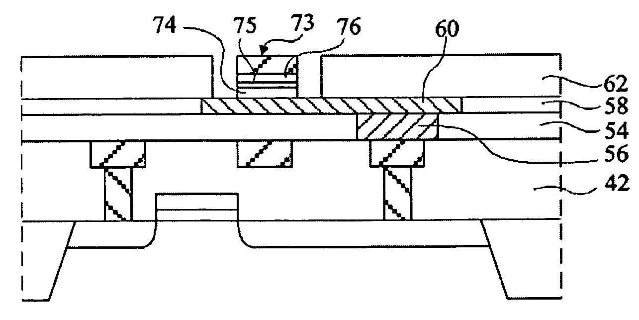
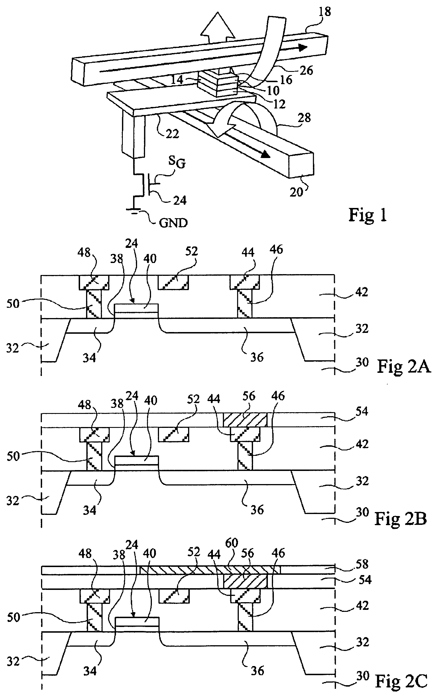
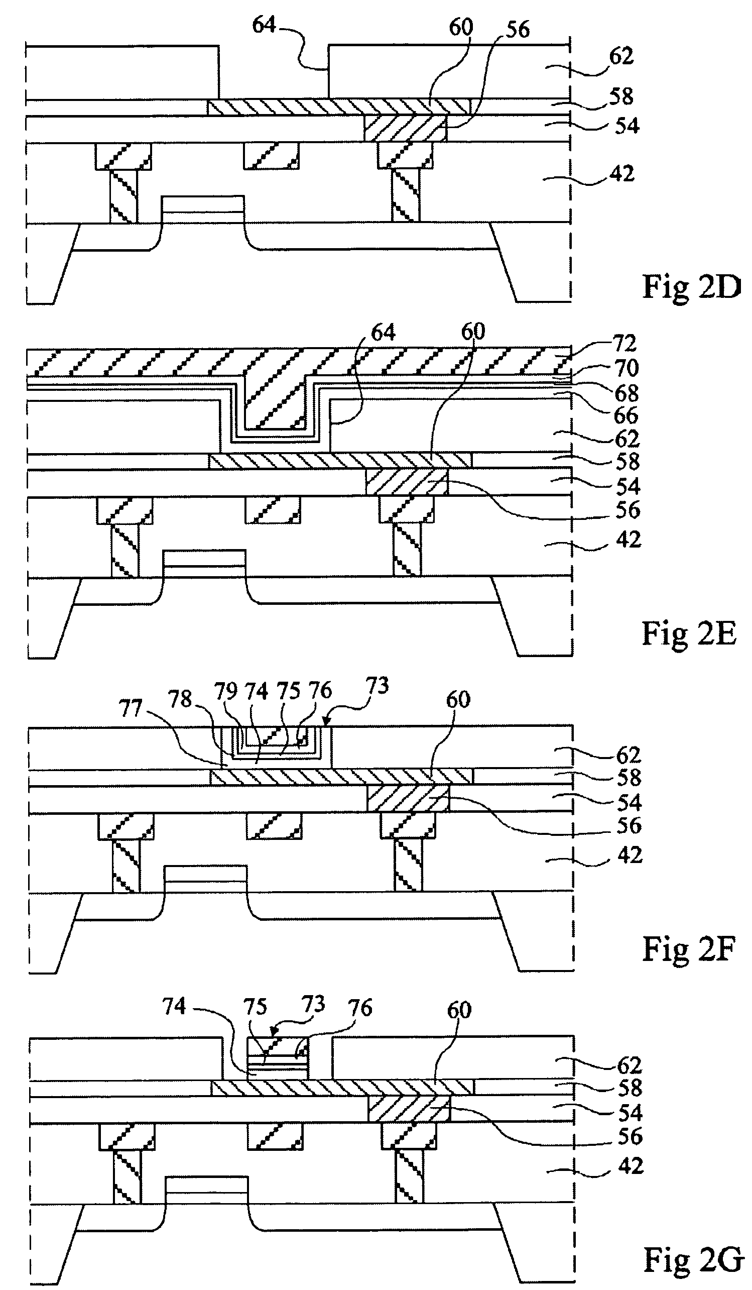
[0033] For clarity, the same elements have been designated with the same reference numerals in the different drawings and, further, as usual in the representation of integrated components, the various drawings are not to scale.

[0034] A first example of a process according to the present invention for manufacturing a magnetic RAM memory element will now be described in relation with FIGS. 3A to 3E. The initial steps of the first method example correspond to the steps previously described in relation with FIGS. 2A to 2D.

[0035]FIG. 3A shows the structure obtained after having deposited, for example, by vapor phase deposition, a layer 80 of a magnetic material, for example, cobalt, on insulating layer 62 and in recess 64. Magnetic layer 80 penetrates into recess 64 to be in contact with connection portion 60. According to a variation of the present invention, insulating layers 58 and 62 correspond to a single insulating layer which is deposited after forming of connection portion 60. ...


PUM


Abstract

A memory element for a magnetic RAM, having a first magnetic portion in a first recess of a first insulating layer; and a non-magnetic portion and a second magnetic portion in a second recess of a second insulating layer covering the first insulating layer, the second recess exposing the first magnetic portion and a portion of the first insulating layer around the first magnetic portion, the non-magnetic portion being interposed between the first and second magnetic portions.

Description

BACKGROUND OF THE INVENTION [0001] 1. Field of the Invention [0002] The present invention relates to a magnetic random access memory or MRAM and a method for manufacturing such a memory. [0003] 2. Discussion of the Related Art [0004]FIG. 1 illustrates the operation of a magnetic RAM. Such a memory comprises an array of memory elements arranged in rows and in columns, a single memory element 10 being shown in FIG. 1. Each memory element 10 is formed of the stacking of three layers: a first layer 12 formed of a magnetic material, for example, cobalt, having a fixed magnetic orientation, a second layer 14 formed of an insulator, and a third layer 16 formed of a ferromagnetic material, for example, cobalt and iron alloy or a nickel and iron alloy, the magnetic orientation of which can vary. Insulating layer 12 behaves as a barrier to prevent the alloying between magnetic layer 12 and ferromagnetic layer 16 and enable the passing of electrons, the spin of which must be kept. Generally, e...

Claims


Application Information

Patent Timeline
Patent Type & Authority Applications(United States)
IPC IPC(8): H01L29/94
CPCH01L43/12B82Y10/00G11C11/16H01L27/228G11C11/1675H10B61/22H10N50/01
Inventor BOIVIN, PHILIPPE
Owner STMICROELECTRONICS (ROUSSET) SAS
Why Eureka
Try Eureka