Method to fabricate discreet vertical transistors

a vertical transistor and transistor technology, applied in semiconductor devices, digital storage, instruments, etc., can solve the problems of low junction leakage current in sic substrate devices, random device characteristics, undesirable short channel effects of transistors,

Active Publication Date: 2017-09-28
WESTERN DIGITAL TECH INC
View PDF1 Cites 3 Cited by
  • Summary
  • Abstract
  • Description
  • Claims
  • Application Information

AI Technical Summary

Problems solved by technology

Amorphous silicon (a-Si) based thin film transistors (TFT) have been used to improve transistor performance; however, these transistors have undesirable short channel effects and randomness in device characteristics.
Therefore, junction leakage currents in SiC substrate devices are very ...

Method used


Image

  • Method to fabricate discreet vertical transistors
  • Method to fabricate discreet vertical transistors
  • Method to fabricate discreet vertical transistors

Examples


Embodiment Construction

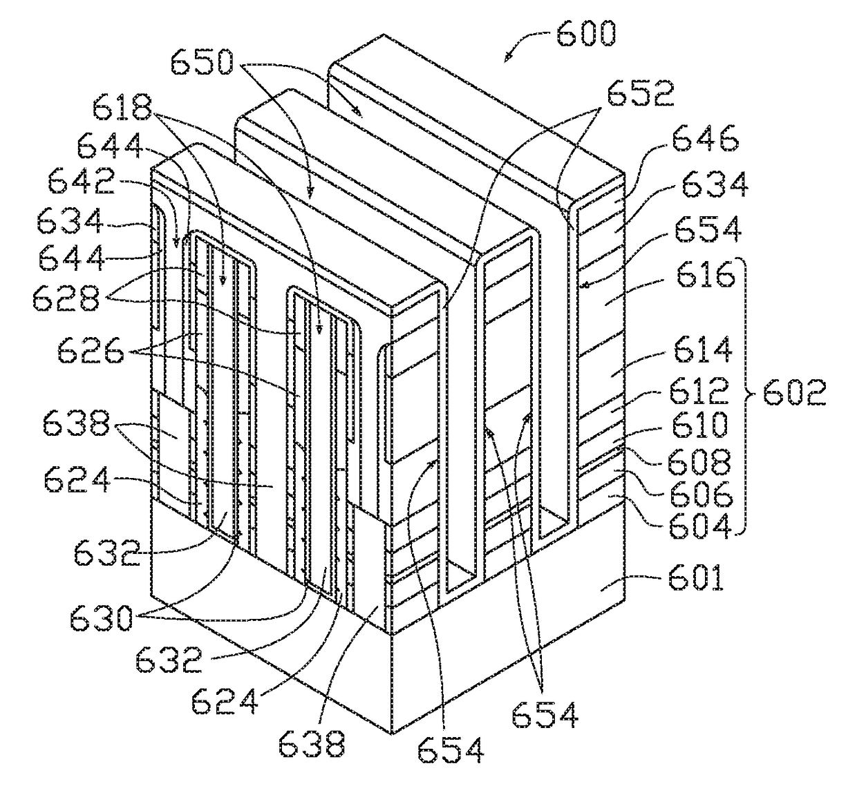
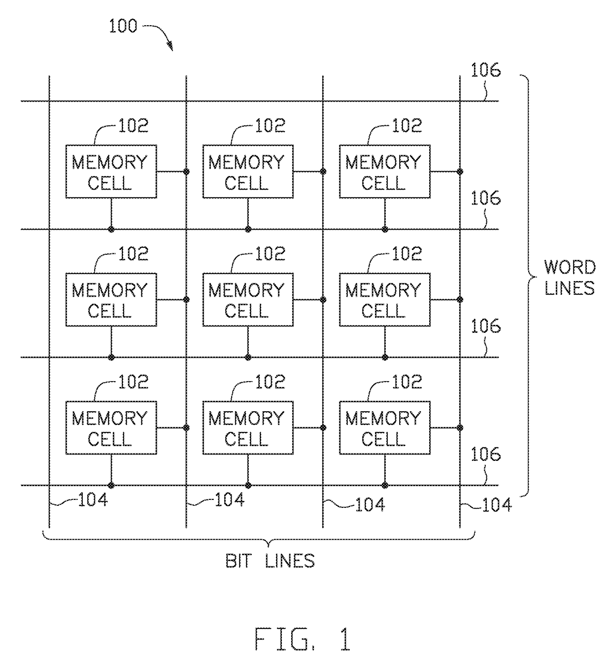
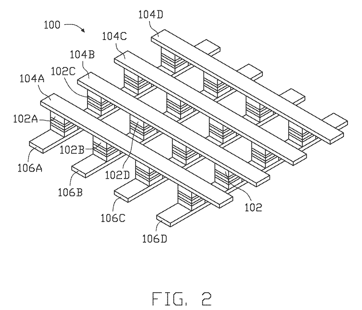
[0021]In the following, reference is made to embodiments of the disclosure. However, it should be understood that the disclosure is not limited to specific described embodiments. Instead, any combination of the following features and elements, whether related to different embodiments or not, is contemplated to implement and practice the disclosure. Furthermore, although embodiments of the disclosure may achieve advantages over other possible solutions and / or over the prior art, whether or not a particular advantage is achieved by a given embodiment is not limiting of the disclosure. Thus, the following aspects, features, embodiments and advantages are merely illustrative and are not considered elements or limitations of the appended claims except where explicitly recited in a claim(s). Likewise, reference to “the disclosure” shall not be construed as a generalization of any inventive subject matter disclosed herein and shall not be considered to be an element or limitation of the ap...


PUM


Abstract

The present disclosure generally relates to the fabrication of metal-oxide-semiconductor (MOS) select transistors in a vertical orientation such that the transistor pair fits within the footprint of a 4F2 memory cell. The present disclosure further relates to the simultaneous fabrication of a vertical stack of transistors in which each transistor is distinct, as opposed to being serially connected in a NAND-like string. An initial stack of materials is built to include silicon layers to act as source and drain regions as well as to serve as epitaxial growth seed points. As such, the transistor disclosed may be utilized in conjunction with memory elements such as Phase Change, Resistive, or Magnetic RAM memory within array designs, among others.

Description

BACKGROUND OF THE DISCLOSURE[0001]Field of the Disclosure[0002]Embodiments of the present disclosure generally relate to data storage and computer memory systems, and more particularly to metal-oxide-semiconductor (MOS) select transistors formed in a vertical orientation.[0003]Description of the Related Art[0004]Memory devices are typically provided as internal, semiconductor, integrated circuits in computers or other electronic devices. Many types of memory exist including random access memory (RAM), read only memory (ROM), dynamic random access memory (DRAM), synchronous dynamic random access memory (SDRAM), and flash memory; however, each is useful only for 2-D memory fabrication or they are serially connected and, as such, must operate similarly to NAND flash strings.[0005]Flash memory devices have developed into a common source of non-volatile memory for a wide range of electronic applications. Flash memory devices typically use a one-transistor memory cell that allows for high...

Claims


Application Information

Patent Timeline
IPC IPC(8): H01L45/00H01L43/12H01L43/02H01L27/24
CPCH01L45/1206H01L27/2454H01L45/1675H01L43/02H01L45/1233H01L43/12G11C11/1659G11C2213/74H10B61/22H10B63/34
Inventor APODACA, MAC D.SHEPARD, DANIEL ROBERT
Owner WESTERN DIGITAL TECH INC
Why Eureka
Try Eureka