Magnetic RAM and its data reading method

A memory, random access technology, applied in static memory, digital memory information, information storage, etc., can solve the problem of impossible to fully improve the integration density of MTJ components, increase in chip size, etc.

Inactive Publication Date: 2004-10-06
KK TOSHIBA
View PDF4 Cites 3 Cited by
  • Summary
  • Abstract
  • Description
  • Claims
  • Application Information

AI Technical Summary

Problems solved by technology

[0043] However, if the number of cell arrays is simply increased while reducing the number of cells connected to the bit line BL due to constraints on the maximum number of cells connectable to the bit line BL, the chip size increases and it is impossible to sufficiently increase the Integration density
Therefore, it is almost impossible to take the above measures for mass storage

Method used


Image

  • Magnetic RAM and its data reading method
  • Magnetic RAM and its data reading method
  • Magnetic RAM and its data reading method

Examples


Embodiment Construction

[0121] 1. Outline of the present invention

[0122] An overview of a magnetic random access memory according to an embodiment of the present invention is provided below.

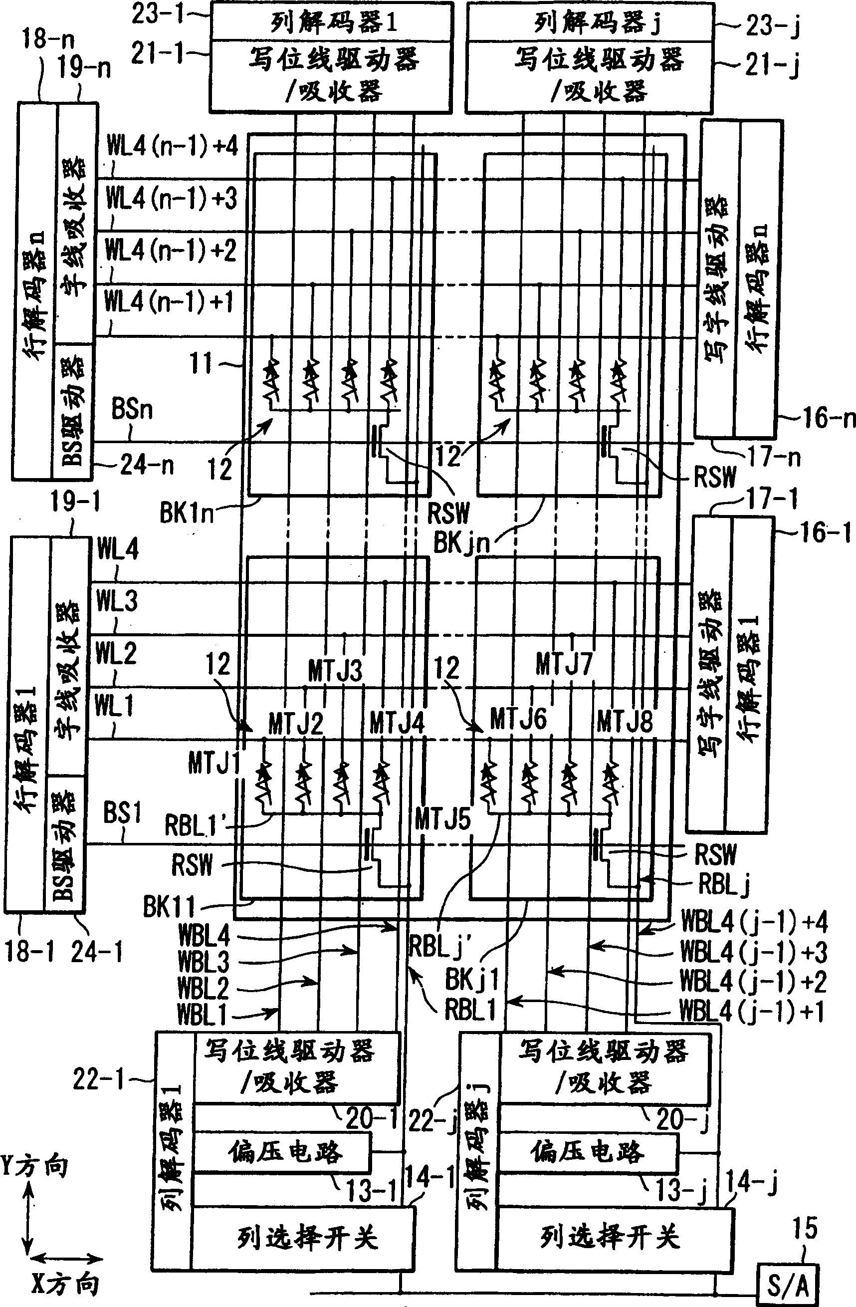
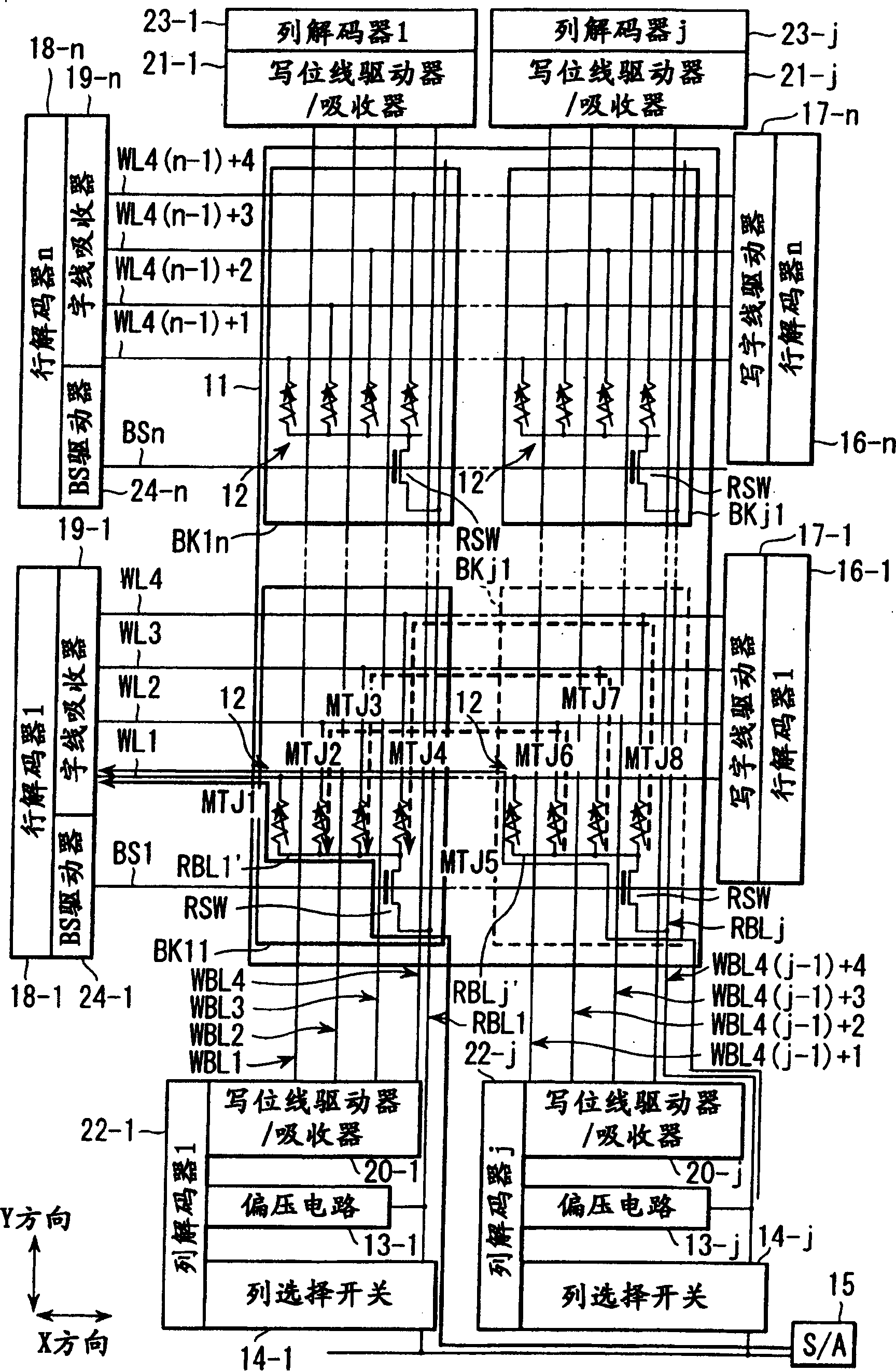
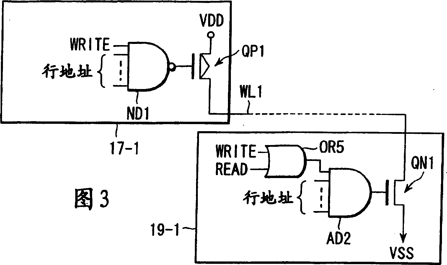
[0123] First, a magnetic random access memory (MRAM) according to an embodiment of the present invention uses [1] wherein one read switch element is shared by a plurality of MTJ (magnetic tunnel junction) elements, and the plurality of MTJ elements are aligned in a direction perpendicular to the surface of the semiconductor substrate (vertical direction) are stacked in multiple stages to form a module structure, [2] in which one read switch element is shared by multiple MTJ elements, and multiple MTJ elements are in a direction parallel to the surface of the semiconductor substrate (lateral direction) arranged to form a module structure, or [3] in which two read switch elements are shared by a plurality of MTJ elements arranged in a direction (lateral) parallel to the surface of the semiconductor substrate t...


PUM


Abstract

A magnetic random access memory having a memory cell array in which one block is formed from a plurality of magnetoresistive elements using a magnetoresistive effect, and a plurality of blocks are arranged in row and column directions, includes a plurality of first magnetoresistive elements arranged in a first block, a plurality of first word lines each of which is independently connected to one terminal of a corresponding one of the first magnetoresistive elements and runs in the row direction, a first read sub bit line commonly connected to the other terminal of each of the first magnetoresistive elements, a first block select switch whose first current path has one end connected to one end of the first read sub bit line, and a first read main bit line which is connected to the other end of the first current path and runs in the column direction.

Description

[0001] Cross References to Related Patent Applications [0002] This application is based on and claims priority from prior Japanese Patent Application No. 2002-374716 filed on December 25, 2002, the entire contents of which are hereby incorporated by reference. technical field [0003] The present invention relates to a magnetic random access memory (MRAM) for storing "1" and "0" data by using a magnetoresistive effect. Background technique [0004] In recent years, many memories utilizing new principles for storing data have been proposed. One of them is a magnetic random access memory (MRAM) utilizing a tunneling magnetoresistance (hereinafter referred to as TMR) effect. As a proposal on a magnetic random access memory, for example, the following non-patent reference 1 is known: Roy Scheuerlein et al., "A 10ns Read and Write Non-Volatile Memory Array Using a Magnetic Tunnel Junction and FET Switch in each Cell", 2000 ISSCC Digest of Technical Papers (U.S.A.), February 2...

Claims


Application Information

Patent Timeline
Patent Type & Authority Applications(China)
IPC IPC(8): G11C11/15H01L21/8246H01L27/105H01L43/08
CPCG11C11/15
Inventor 岩田佳久
Owner KK TOSHIBA
Why Eureka
Try Eureka