Directed assembly of highly-organized carbon nanotube architectures
a carbon nanotube and architecture technology, applied in the field of carbon nanotubes, can solve the problems of complicated nanotube fabrication methods, inability to grow nanotubes in more than, and difficulty in obtaining nanotubes that are exclusively oriented parallel to the substrate in predetermined orientations
- Summary
- Abstract
- Description
- Claims
- Application Information
AI Technical Summary
Problems solved by technology
Method used
Image
Examples
first embodiment
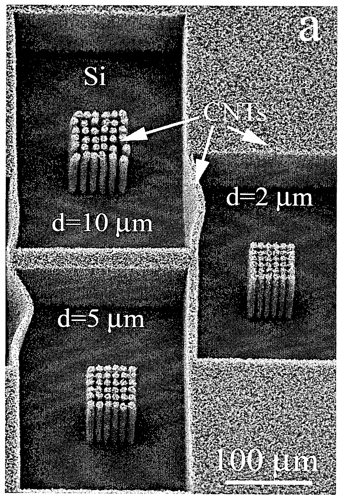
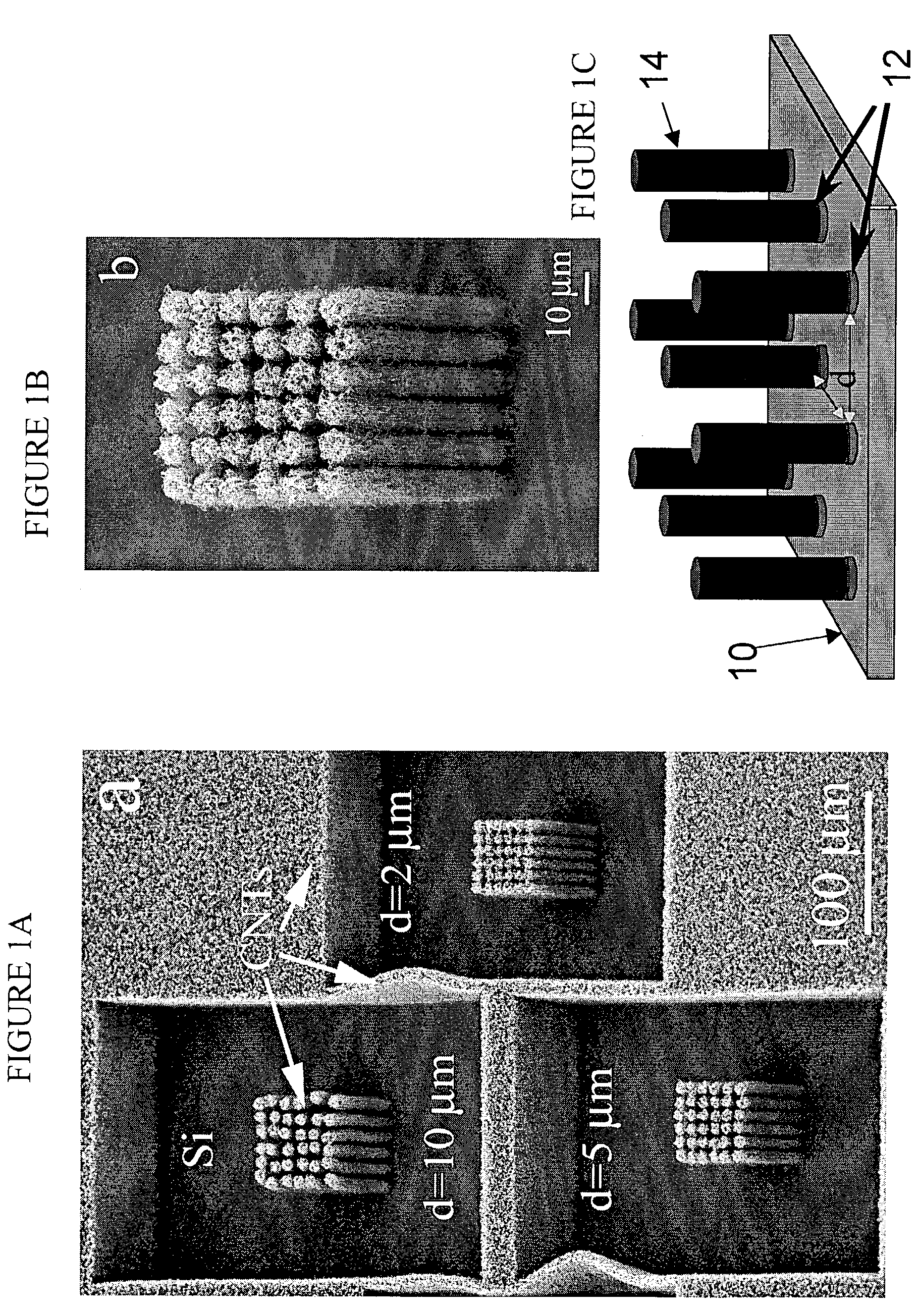
[0029]FIGS. 1A–B show a striking example of aligned nanotube pillars placed on specific sites on the substrate according to one aspect of the FIG. 1A illustrates an SEM image of pillars of aligned carbon nanotube (CNT) arrays within trenches surrounded by a thick aligned nanotube film grown vertically on the SiO2 pattern on a Si substrate. The nanotube film was selectively grown on a SiO2 pattern or template structure. In the center of box-like regions defined by the nanotube film walls, micro-sized cylindrical blocks or pillars of vertically oriented nanotubes are grown from the underlying template structure constituted by SiO2 patterns in this case. Within each block, the nanotubes are highly oriented and densely packed. Three different pillar packing densities are shown in FIG. 1A, where the separation between pillars in each group is 10 microns (top), 5 microns (bottom) and 2 microns (center).
[0030]FIG. 1B is an enlarged image of the middle array shown in FIG. 1A showing the al...
second embodiment
[0037]The porous nanotube films were obtained by using a porous template structure or layer formed over a substrate. For example, a porous silica template layer was obtained by forming a silica layer on the silicon substrate and then photolithographically masking the layer and etching pores or holes in this layer. Since the pores or holes are formed by photolithography and etching, they have a controlled size. The pores or holes extend down to the silicon substrate and may extend into the silicon substrate if desired. Thus, portions of the substrate are exposed through pores in the porous template layer. Nanotube-forming gases or mixtures were provided onto the porous template layer and the carbon nanotubes were selectively grown on the porous template layer. However, the nanotubes were not formed on portions of the substrate exposed through pores in the porous template layer. Furthermore, the nanotubes did not form on the template layer pore sidewalls because the template layer thi...
third embodiment
[0039]The method and structure of the third preferred embodiment will now be described. In the third embodiment, selective nanotube growth on the template structure having at least one, and preferably two or more surfaces. The nanotube growth occurs in a direction normal to the respective surfaces and hence this approach can be harnessed to simultaneously grow nanotubes in several predetermined directions. For example, nanotube growth in mutually orthogonal directions may be carried out by using template structures comprising of deep etched trenches, drilled all the way to silicon substrate, separating several thick SiO2 template structure towers. Preferably, the nanotubes are grown on side surfaces of the template structures, which are preferably thicker than about 200 nm, preferably thicker than 2 microns. For example, the template structure may be several microns thick, such as 2 to 10 microns thick, preferably 5 to 8.5 microns thick. However, thickness of the template structure ...
PUM
| Property | Measurement | Unit |
|---|---|---|
| Length | aaaaa | aaaaa |
| Time | aaaaa | aaaaa |
| Thickness | aaaaa | aaaaa |
Abstract
Description
Claims
Application Information


