Overmolded semiconductor package with an integrated EMI and RFI shield

a technology of shielding and semiconductor devices, applied in semiconductor devices, semiconductor/solid-state device details, electrical devices, etc., can solve the problems of increasing the size of the package, substantially increasing the packaging cost, and undesired increase of the thickness of the final overmolded package by the metal shield

Active Publication Date: 2007-04-03
SKYWORKS SOLUTIONS INC
View PDF3 Cites 132 Cited by
  • Summary
  • Abstract
  • Description
  • Claims
  • Application Information

AI Technical Summary

Benefits of technology

[0010]According to this exemplary embodiment, the overmolded package can further comprise a post situated over the substrate, where the post is connected to the conductive layer. For example, the post can be situated on a solder pad, where the solder pad is connected to a reference voltage. The post can have a width of between approximately 100.0 microns and approximately 200.0 microns, for example. The overmolded package can further comprise a hole situated in the overmold, where the hole is situated over the post, where the hole is filled with the conductive polymer, and where the conductive polymer is in contact with the post. According to one embodiment, the invention is a method for achieving the above-described structure. Other features and advantages of the present invention will become more readily apparent to those of ordinary skill in the art after reviewing the following detailed description and accompanying drawings.

Problems solved by technology

However, semiconductor device manufacturers are challenged to provide effective EMI and RFI shielding for an overmolded semiconductor package without increasing the size of the package and without substantially increasing packaging cost.
As a result, the metal shield undesirably increases the thickness of the final overmolded package.
Also, the formation of the metal shield requires an extra process step and additional materials, which significantly increases packaging cost.
However, the conductive foam or rubber must be applied manually and requires special materials and an extra process, which significantly increases packaging cost.
Additionally, the conductive foam or rubber undesirably increases the thickness of the final overmolded package.

Method used


Image

  • Overmolded semiconductor package with an integrated EMI and RFI shield
  • Overmolded semiconductor package with an integrated EMI and RFI shield
  • Overmolded semiconductor package with an integrated EMI and RFI shield

Examples


Embodiment Construction

[0014]The present invention is directed to overmolded semiconductor package with an integrated EMI and RFI shield. The following description contains specific information pertaining to the implementation of the present invention. One skilled in the art will recognize that the present invention may be implemented in a manner different from that specifically discussed in the present application. Moreover, some of the specific details of the invention are not discussed in order not to obscure the invention.

[0015]The drawings in the present application and their accompanying detailed description are directed to merely exemplary embodiments of the invention. To maintain brevity, other embodiments of the present invention are not specifically described in the present application and are not specifically illustrated by the present drawings.

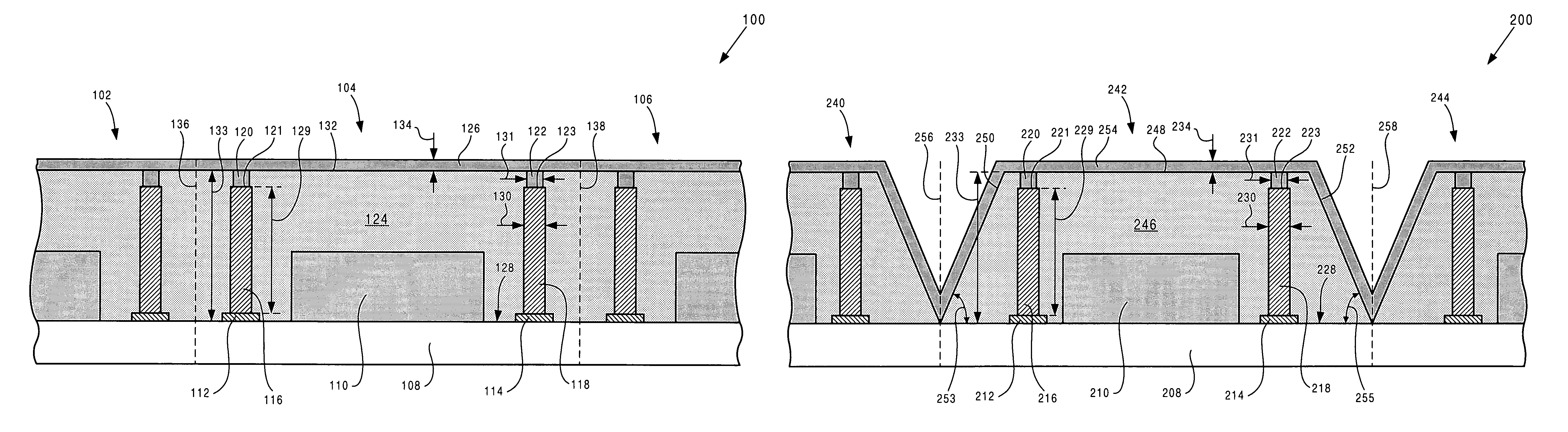
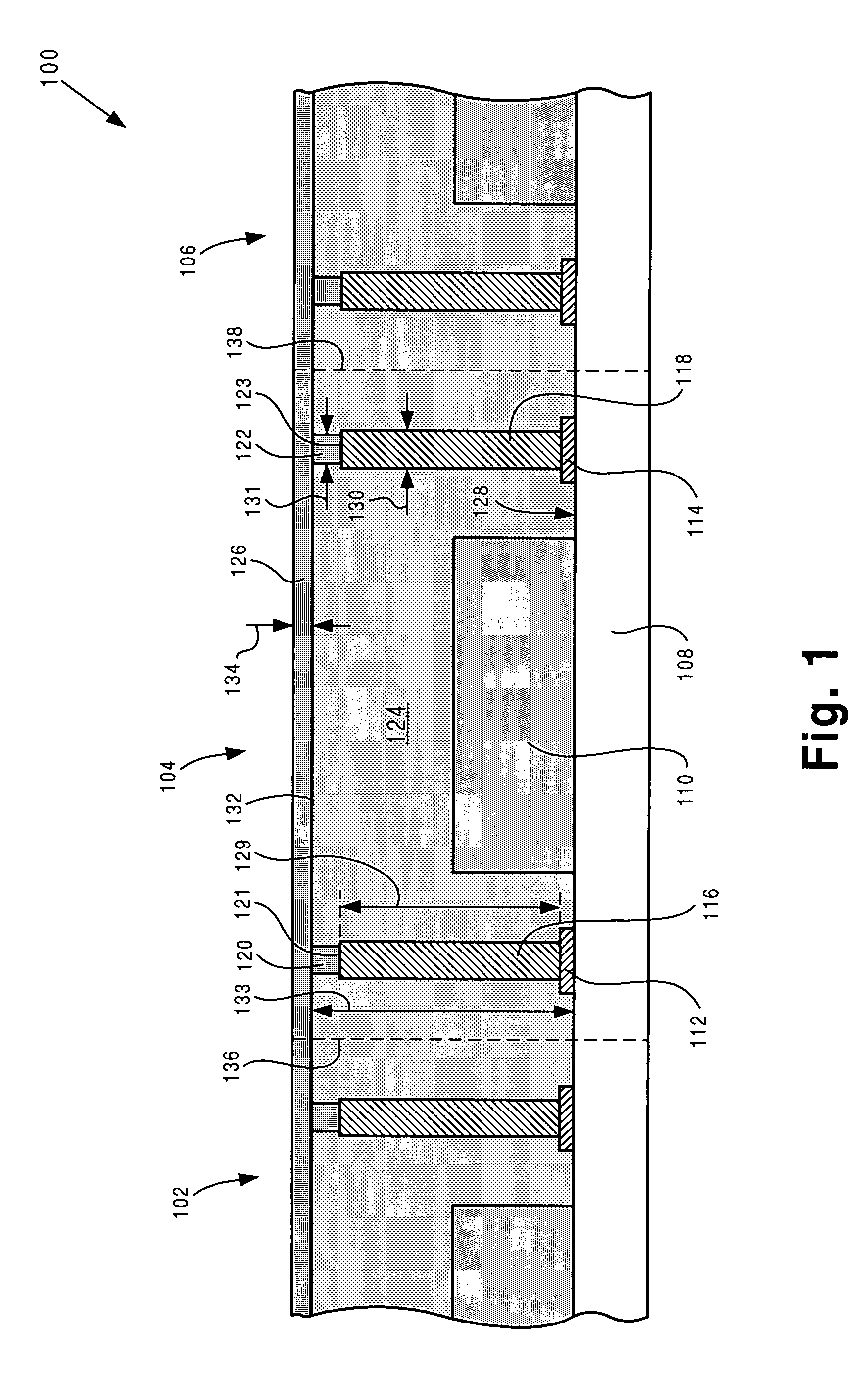
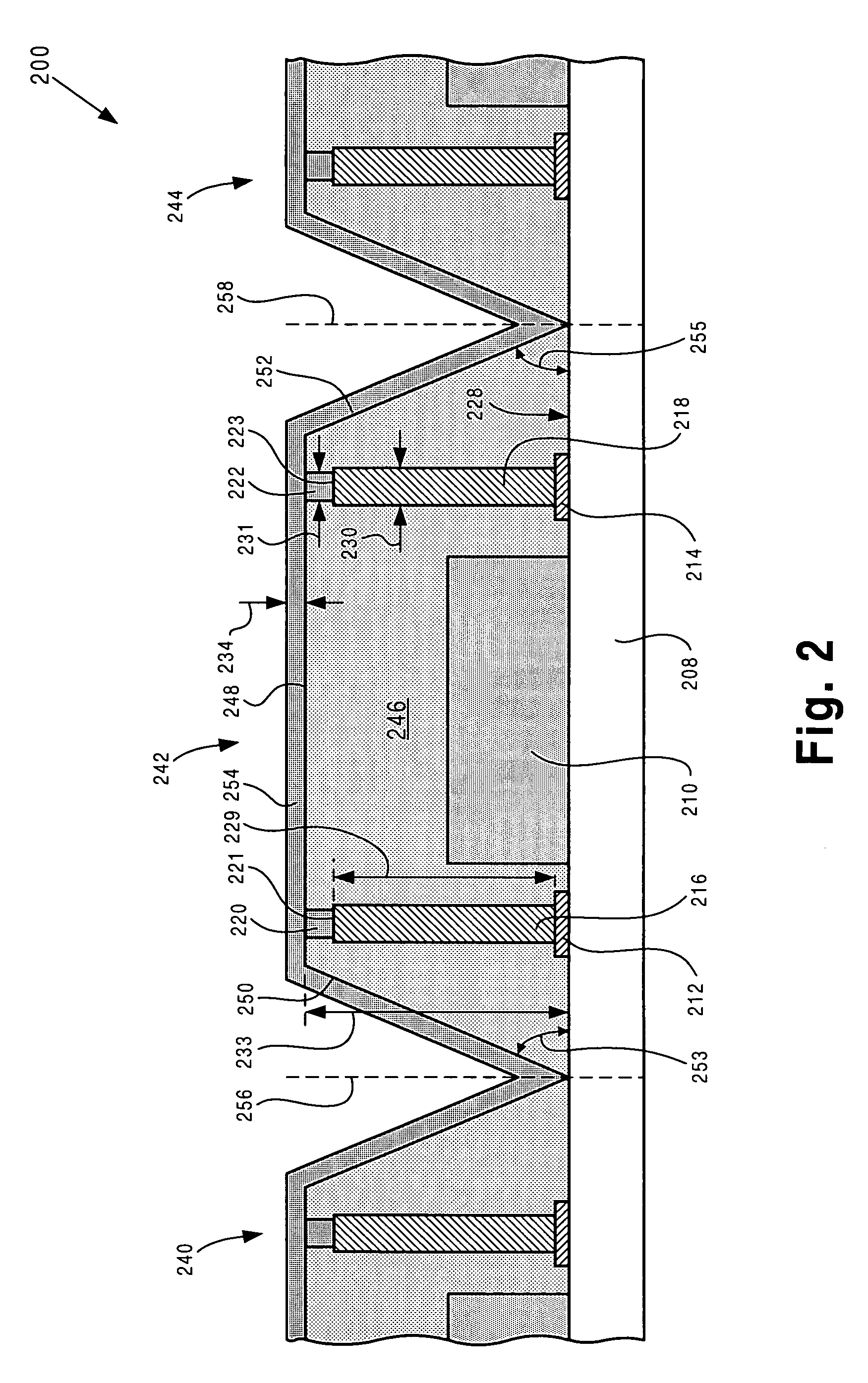
[0016]FIG. 1 shows a cross-sectional view of structure 100, which is utilized to describe one embodiment of the present invention. Certain details and f...


PUM


Abstract

According to one exemplary embodiment, an overmolded package comprises a semiconductor die situated on a substrate. The overmolded package further comprises an overmold situated over the semiconductor die and the substrate, where the overmold has a top surface. The overmolded package further comprises a conductive layer situated on the top surface of the overmold, where the conductive layer comprises a conductive polymer, and where the conductive layer forms an EMI and RFI shield. According to this exemplary embodiment, the overmolded package can further comprise a post situated over the substrate, where the post is connected to the conductive layer. The overmolded package can further comprise a hole situated in the overmold, where the hole is situated over the post, where the hole is filled with the conductive polymer, and where the conductive polymer is in contact with the post.

Description

BACKGROUND OF THE INVENTION[0001]1. Field of the Invention[0002]The present invention is generally in the field of semiconductor device packaging. More specifically, the invention is in the field of shielding of semiconductor device packages.[0003]2. Related Art[0004]Portable electronic devices, such as cell phones, typically utilize multi-component semiconductor modules to provide a high level of circuit integration in a single molded package. The multi-component semiconductor module can include, for example, a semiconductor die and a number of electronic components, which are mounted on a circuit board. The circuit board including the semiconductor die and electronic components can be encapsulated in a molding process to form an overmolded semiconductor package. To ensure an acceptable level of performance in devices such as cell phones, which are required to properly operate in diverse environments, the overmolded semiconductor package must be shielded from Electro-Magnetic Inter...

Claims


Application Information

Patent Timeline
Patent Type & Authority Patents(United States)
IPC IPC(8): H01L21/44H01L23/31H01L23/552
CPCH01L23/552H01L24/97H01L23/3121H01L2924/01004H01L2924/01005H01L2924/01013H01L2924/01029H01L2924/01033H01L2924/01047H01L2924/01078H01L2924/01079H01L2924/19041H01L2924/3025H01L2924/181H01L2924/00H01L23/60
Inventor WARREN, ROBERT W.JAYARAMAN, SURESHPOTTEBAUM, LARRY D.
Owner SKYWORKS SOLUTIONS INC
Why Eureka
Try Eureka